


1. INTRODUCTION
In recent years, metal oxides have attracted significant research interest due to their unique physical and chemical properties. Many of these studies have investigated the characteristics of various metal oxides, and among them, ZnO has received notable attention because of its high luminescent efficiency, optical transparency in the visible region, high electrical conductivity, and gas sensing properties [1-4]. These properties are valuable in various applications such as fluorescent and field-emitting devices, solar cell windows, transparent electrodes, touch display screens, and gas sensors [5-8]. However, ZnO is impacted by the synthesis method used in its creation, and the resulting poor crystallinity of ZnO has a negative effect on the performance of ZnO-based devices, particularly low photosensitivity [9]. Synthesis techniques which can create high-quality ZnO are thus necessary for its continued use. Synthesis techniques employed for this purpose include molecular beam epitaxy (MBE), chemical vapor deposition (CVD), hydrothermal methods, and electrodeposition methods [10-13]. However, MBE and CVD have their own unique drawbacks, including complicated processing, the use of hazardous reagents, equipment costs, high temperatures, and long process times. For hydrothermal and electrodeposition methods, since they require a variety of additives, such as zinc nitrate, hexamethylenetetramine, and potassium chloride, to synthesize the ZnO films, the processes are complex, and the costs are relatively expensive.
Various oxidation methods have recently been considered as alternatives, because of their simplicity, eco-friendly nature, and low equipment costs. Among the known oxidation methods, thermal oxidation and water treatment methods are typical and widely used methods. Thermal oxidation not only makes it easy to prepare ZnO thin film in a short time, but it can also oxidize large surface area Zn film in a uniform manner [14]. High temperatures, however, are essential for the oxidation of Zn film since the metallic Zn can be completely transformed to ZnO at temperatures over 450 ┬░C [15]. Moreover, slow cooling is essential to minimize the appearance of defects after thermal oxidation. In previous studies, Zhang et al. [16] oxidized Zn films at temperatures ranging from 300 to 600 ┬░C using the thermal oxidation method. They observed that Zn films started oxidizing to ZnO thin films at 300 ┬░C, and that ZnO thin films oxidized at 600 ┬░C featured the best crystallinity and strongest UV emission. Avila et al. [17] reported that when the cooling rate was dramatically increased, fragile layers could be formed due to lattice mismatching between the ZnO films and the substrate. Therefore, it was difficult to fabricate ZnO-based transparent and flexible devices by thermal oxidation due to the low melting point of most polymer substrates. Water treatment, which is a simple, low-temperature, cost-effective, scalable, and eco-friendly method, can overcome almost all the limitations of conventional synthesis techniques and make it possible to use flexible polymers with limited thermal stability as substrates [18, 19]. Unfortunately, the water treatment method still has the critical drawback of requiring long oxidation times to synthesize high-quality ZnO thin film. According to Shanmugan et al. [20], when an In2O3 film was prepared using a hot water treatment method with various processing times, mixed phases were formed at short processing times of below 5 hours, and a single cubic In2O3 phase was formed after oxidation time of at least 12 hours. Tan et al. [21] reported that when etched Zn foils were oxidized by hot water treatment, prolonged treatment times (~24 h) were essential to obtaining ZnO thin films.
Considering these factors, we suggest a new oxidation method, named the electrochemical oxidation (ECO) method, to synthesize high-quality ZnO thin films at low temperatures and short oxidation times. The ECO method is affected by a variety of factors, including the temperature of the DI water, pH values, current density, and process times. In previous studies, ZnO films were oxidized using the ECO method at various current densities, ranging from 0.2 to 2 mA┬Ęcm-2. The ZnO film oxidized at 1 mA┬Ęcm-2 showed the strongest intensity of ZnO (002) peak and near-band-edge (NBE) emission [22]. When small amounts of NaOH (0.02 g) were added to the solution to control the pH values, the Zn film peeled off from the Si substrate as soon as the experiment began. This indicated that it was impossible to oxidize a Zn film deposited on a Si substrate using the ECO method in aqueous solution containing OH- ions.
In this study, to find the optimal temperature of DI water, we oxidized Zn films using the ECO method in DI water at various temperatures, ranging from 30 to 90 ┬░C, at 1 mA┬Ęcm2 for a short oxidation time of 1 h. The effects of the DI water temperature on the structural and optical properties of ZnO thin films were investigated, and a mechanism for the ECO method was proposed.
2. EXPERIMENTAL PROCEDURES
Prior to depositing metallic Zn onto highly doped p-type Si (100) substrates (0.005 Ōä”┬Ęcm, 18 ├Ś 36 mm2), the Si substrates were cleaned using piranha solution (95% H2SO4 : 30% H2O2 = 4 : 1) at 90 ┬░C for 15 min. Subsequently, these substrates were immersed in a 5% hydrofluoric acid solution for 1 min to remove residual impurities and the native oxide layer. They were then ultra-sonicated in acetone and ethanol for 10 min, respectively. The cleaned substrates were then rinsed with DI water for 2 min and dried with N2 gas. The prepared substrates were placed in a reaction chamber after being fixed on a substrate holder with a mask (18├Ś18 mm2), and the Zn metal source (99.999%) was placed on a tungsten boat in the reaction chamber after being cleaned with acetone to remove surface impurities. The distance between the substrates and Zn source was 13 cm. The chamber pressure was dropped to 1.47 Pa using a rotary pump and then dropped to 2.7 ├Ś 10-3 Pa using a turbomolecular pump. While the Zn metal source was evaporated by heating the tungsten boat and deposited onto Si (100) substrates, the pressure in the reaction chamber was maintained at 2.7 ├Ś 10-3 Pa. The obtained Zn films, which had a thickness of approximately 300 nm and dimensions of 18├Ś18 mm2, were then vacuum-heated in a furnace at 150 ┬░C for 20 min to improve adhesion between the Zn films and the substrates. The vacuum-heated Zn films were then cooled at 2 ┬░C/min to prevent them from cracking under strain.
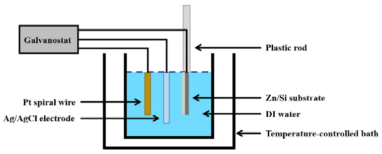
The Zn films deposited on Si substrates were oxidized using the ECO method at various DI water temperatures (30, 50, 70, and 90 ┬░C) for 1 h as shown in the schematic of Fig 1. The galvanostat (Digi-Ivy, DY2100B) used in the ECO process consisted of an anode, cathode, and reference electrode; the Zn films deposited on the Si substrates and a Pt spiral wire were connected as the cathode and anode, respectively, and the reference electrode was composed of Ag/AgCl. A constant-temperature water bath increased the temperature of the DI water up to the corresponding temperature and maintained it thereafter. The distance between the Zn film and Pt spiral wire was maintained at ~8 cm, and they were immersed in a 500 ml beaker filled with DI water without any additives. Subsequently, the potential was automatically changed to fix the current density at 1 mA┬Ęcm-2 using a potentiostat, and the average value of potential was approximately -0.05 V. The Zn film and Pt spiral wire became negatively and positively charged respectively due to their potential difference.
The surface morphologies and structural properties of the ZnO thin films were investigated using field emission scanning electron microscopy (FE-SEM; TESCAN MIRA3 LM) and X-ray diffraction (XRD; PANalytical XŌĆÖPert Pro, Almelo, the Netherlands), respectively. To analyze the optical properties, photoluminescence (PL) spectra of the ZnO thin films were measured in the wavelength range of 350ŌĆō700 nm using a He-Cd laser (325 nm) with an excitation power of 20 mW and a 0.75-m single grating monochromator with a photomultiplier tube.
3. RESULTS AND DISCUSSION
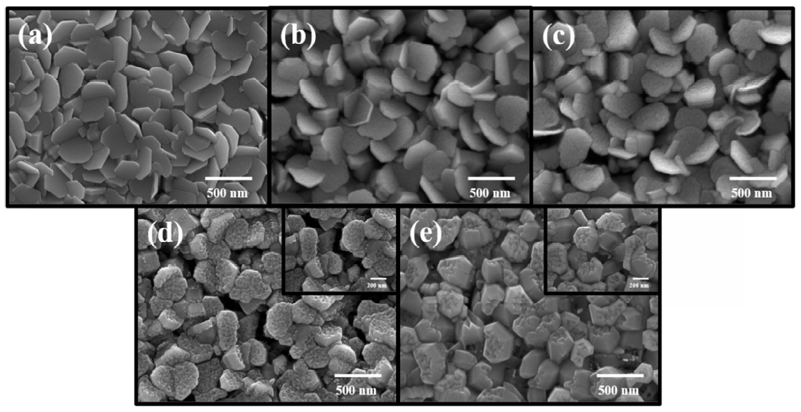
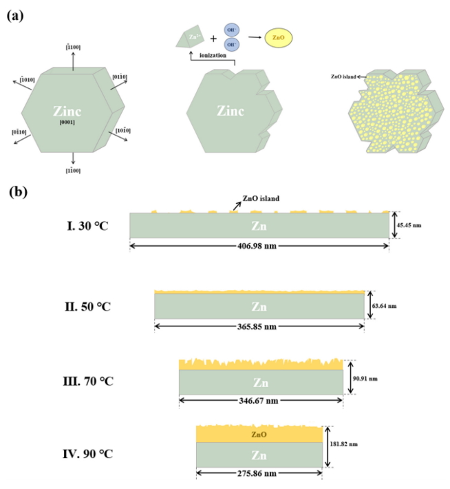
The surface morphologies of the as-deposited Zn film and ZnO thin films oxidized in DI water at 30, 50, 70 and 90 °C using the ECO method for 1 h are shown in Fig 2. As shown in Fig 2 (a), the as-deposited Zn films consisted of typical disk-shaped plates. Compared with the as-deposited Zn film, there were no significant changes in the plate surfaces when Zn films were oxidized in DI water at 30 or 50 °C, indicating that the Zn films were hardly oxidized in the relatively low temperature DI water. By comparison, the surfaces of the disk-shaped plates changed considerably at higher DI water temperatures of 70 and 90 °C. In order to observe the plate surfaces in greater detail, higher-magnification images of ZnO thin films oxidized at these temperatures are shown in the insets of Fig 2 (d) and (e), respectively. In the case of ZnO thin film oxidized at 70 °C, Zn2+ ions, which were ionized from the side surfaces of the Zn plates, combined with OH- ions, and numerous nano-scale ZnO islands were randomly formed on the plate surfaces, resulting in uneven plate surfaces. When the DI water temperature was increased from 70 to 90 o C, more nano-scale ZnO islands became densely stacked on the disk-shaped plate surfaces, and the surface became smooth. In general, Zn, similar to ZnO, has a hexagonal structure which consists of a pair of {0001} planes and six side surfaces including (1 ¯ 1 ¯ 1 ¯ 1 ¯ 1 ¯ 1 ¯
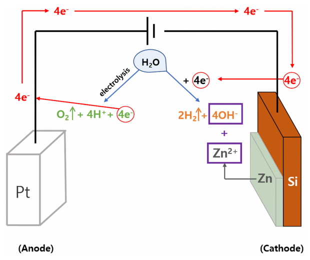
These FE-SEM images revealed that ZnO thin film can be obtained using the ECO method. We subsequently investigated the chemical reactions of Zn film in DI water to clearly define the mechanism of this ECO method, which is carried out in DI water. When a Zn film was immersed in DI water without any additives, Zn2+ ions were ionized from the side surfaces of the disc-shaped Zn plates due to the high degree of ionization, and two electrons were released (Eq. (1)). Zn2+ ions move freely in DI water, and the electrons react with H2O molecules and the dissolved oxygen, which induces OH- ions near the Zn film (Eqs. (2) and (3)). Subsequently, OH- ions combine with the Zn2+ ions, forming ZnO on the Zn surfaces (Eq. (4)) [28, 29].
Although the Zn film was ionized to Zn2+ ions when immersed in DI water, in the ECO process, the main factor for Zn film ionization is the potential difference between the anode and cathode (Eq. (5)). Moreover, Zn2+ ions ionized without an electrochemical system move freely in DI water, while the Zn2+ ions generated by the ECO process are immediately trapped in the vicinity of the negatively charged Zn film, increasing the combination rate between Zn2+ ions and OH- ions. At the same time, the electrolysis of H2O occurs near the Pt spiral wire, and the generated electrons move to the cathode through the leading wire (Eq. (6)). H2O molecules close to cathode react with the electrons that are continuously supplied from the negative pole and derived from the ionization of Zn, producing an ample amount of OH- ions (Eq. (7)). A large amount of OH- ions immediately combines with Zn2+ ions captured near the cathode, forming Zn(OH)2, and ZnO is produced by the thermal decomposition of Zn(OH)2 (Eqs. (8) and (9)) [30]. Therefore, when the Zn film was oxidized using the ECO method, ZnO rapidly formed due to the combination of Zn2+ ions captured near the cathode and the prevalence of OH- ions. The oxidation of Zn followed the mechanism of the ECO method, which differs from the above mechanism, as outlined in Eqs. (5) ŌĆō (9). The overall chemical reactions in the ECO process are illustrated in Fig 4.
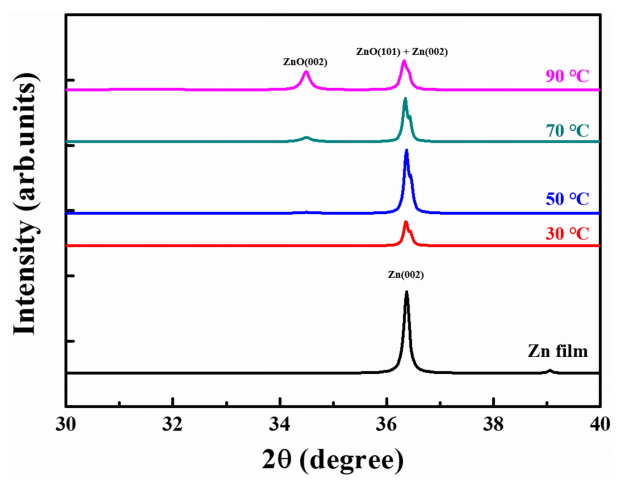
XRD analysis was carried out to investigate the effect of the temperature of DI water on the variation in crystal structure from Zn to ZnO. Fig 5 presents the XRD patterns of the Zn film and ZnO thin films oxidized in DI water at 30, 50, 70, and 90 ┬░C. The Zn film has a strong diffraction peak located at around 36.3 ┬░ corresponding to the Zn (002) plane, which indicates that the Zn film was hardly oxidized. The ZnO thin films oxidized at various temperatures of DI water feature two diffraction peaks, observed at approximately 34.4 ┬░ and 36.4 ┬░, respectively. Among the two diffraction peaks, a weak diffraction peak located at 34.4 ┬░ corresponds to the ZnO (002) plane, and the distinct diffraction peak located at 36.4 ┬░ is attributed to the overlap of diffraction peaks from the ZnO (101) and Zn (002) planes due to their similar diffraction angles [31]. We fitted the diffraction peaks observed at 34.4 ┬░ by using the Lorentzian function to distinguish the intensity of the diffraction peak from the ZnO (101) plane. As shown in Table 1, the intensity of the ZnO (002) peak gradually increased, and the intensity of the ZnO (101) peak increased as the temperature of the DI water increased from 30 to 50 ┬░C but gradually decreased at DI water temperatures of over 50 ┬░C. The lowest intensity ZnO (002) and ZnO (101) peaks appeared in the ZnO thin film oxidized at 30 ┬░C, because it was hardly oxidized given the very low temperature of DI water. When the temperature of DI water was increased to 50 ┬░C, the intensity of the ZnO (002) and ZnO (101) peaks increased due to the formation of a higher amount of nano-scale ZnO islands, which were dependent on the increased DI water temperature. However, although the amount of nano-scale ZnO islands increased as the DI water temperature increased from 50 to 90 ┬░C, the intensity of the ZnO (101) peak decreased because the nanoscale ZnO islands began to stack on the disk-shaped plates, especially in the (0001) plane. The formation of nano-scale ZnO islands on the (0001) plane could be verified by the increased intensity of the ZnO (002) peak, which indicated that at temperatures over 50 ┬░C, ZnO was preferentially formed along the direction perpendicular to the substrate. In general, the full width at half maximum (FWHM) of the diffraction peak from the ZnO (002) plane and the residual stress of the ZnO thin film were used to assess the crystallinity of the ZnO thin film. The residual stress of the ZnO thin film was calculated using the following equation [32]:
where ŌĆśŽāŌĆÖ is the stress, Cij is the elastic stiffness constants for ZnO (i.e., C11 = 209.7, C12 = 121.1, C13 = 105.1, and C33 = 210.9 GPa), ŌĆścŌĆÖ is the lattice constant, and ŌĆśc0ŌĆÖ is the strainfree lattice parameter of the ZnO thin film [33]. The FWHM value significantly diminished from 1.13 ┬░ to 0.23 ┬░ as the DI water temperature increased from 30 to 70 ┬░C. The ZnO thin film oxidized at 90 ┬░C had the lowest FWHM value (0.17 ┬░). In terms of residual stress, all samples had positive stress values (indicating tensile stress), and the stress value decreased from 0.54 to 0.05 GPa due to a decrease in lattice mismatching as the ZnO film thickness increased. When the thickness of the ZnO thin film increased enough, the lattice mismatch between the Zn film and the ZnO thin film decreased, whereas low thickness ZnO thin film caused greater lattice mismatching [34]. In other words, the reduction in FWHM and residual stress indicated that the crystallinity of the ZnO thin film was improved by increasing the DI water temperature. The ZnO thin film with the lowest FWHM (0.17 ┬░) and residual stress (0.05 GPa) exhibited the best crystallinity.
Fig 6 (a) shows the room temperature PL spectra of ZnO thin films oxidized at various DI water temperatures, showing that all samples exhibit similar PL spectra characterized by a strong NBE emission observed at around 370 nm and a broad deep-level (DL) emission found at approximately 560 nm. The NBE emission is generated by the recombination of electrons and holes to form excitons, while the DL emission is generated by structural defects such as interstitial oxygen, interstitial zinc, oxygen vacancies, and zinc vacancies [35]. In all of the ZnO thin films, the intensity of the NBE emission gradually increased until the DI water temperature reached its highest temperature (90 ┬░C). This was due to the fact that the amount of nano-scale ZnO islands increased with increasing DI water temperature as mentioned previously. In addition, the NBE peak position of the ZnO thin film was red-shifted from 368 to 374 nm due to the decrease in residual stress [36]. In the case of the DL emission, a weak broad green emission was observed in all samples, which is associated with structural defects such as oxygen vacancies and interstitial zinc atoms. However, many studies have reported that high-intensity green emissions are frequently observed in ZnO thin films fabricated by conventional solution-based methods, and these emissions are attributed to oxygen vacancies [37-39]. Therefore, we theorize that in the ECO process, oxygen generated by H2O electrolysis decreased the number of structural defects caused by oxygen vacancies, which led to the lower intensity of this green emission. The intensity ratio of the NBE emission to that of the DL emission peak (INBE/IDL) in the ZnO thin film was plotted as a function of the DI water temperature, in order to evaluate their crystal quality. The INBE/IDL value gradually increased from 0.63 to 3.83 as the temperature increased from 30 to 70 ┬░C, and the ZnO thin film oxidized at 90 ┬░C had the highest INBE/IDL value of 20.53. In other words, when the ZnO thin film was fabricated using the ECO method at 90 ┬░C, we obtained ZnO thin films with a relatively low number of oxygen vacancies and improved structural and optical properties.
4. CONCLUSIONS
We have developed a new oxidation method, named the ECO method, to synthesize high-quality ZnO thin film at low temperature with short processing times. We first investigated the oxidation mechanism of Zn film using the ECO method. The main factor of the fast oxidation rate was determined to be the constant current flow to both the cathode and anode. Zn2+ ions were captured near the cathode (Zn film) and the increased generation rate of both Zn2+ and OH- formed numerous nano-scale ZnO islands on the Zn film surface. As a result of this process, high-quality ZnO thin film was successfully obtained in DI water at 90 ┬░C for 1 h. These results confirm that, unlike conventional oxidation methods, the ECO method can make high-quality ZnO thin film at low oxidation temperatures in a short amount of time. Therefore, the ECO method is expected to be promising route to the low-cost fabrication of transparent and flexible optoelectronic devices using high-quality ZnO thin films.