Thermoelectric Performance of Sn and Bi Double-Doped Permingeatite
Article information
Abstract
In this study, mechanical alloying was performed to synthesize permingeatite Cu3Sb1-x-ySnxBiySe4 (0.02 ≤ x ≤ 0.06 and 0.02 ≤ y ≤ 0.04) doped with Sn and Bi. Hot pressing was subsequently conducted to achieve dense sintered bodies. When the Bi content was constant, the carrier concentration increased with the Sn content, but the mobility decreased owing to the increased carrier concentration. In contrast, when the Sn content was constant, the carrier concentration and mobility were not significantly affected by the Bi content. Higher electrical conductivity was observed in specimens with a higher Sn content or lower Bi content; consequently, Cu3Sb0.92Sn0.06Bi0.02Se4 exhibited the highest electrical conductivity. The Seebeck coefficient increased with temperature, and it is inferred that the permingeatite doped with Sn/Bi does not undergo an intrinsic transition until 623 K. In contrast to the electrical conductivity, a higher Seebeck coefficient was obtained in the specimens with a lower Sn content or higher Bi content; consequently, Cu3Sb0.94Sn0.02Bi0.04Se4 exhibited the highest Seebeck coefficient. Cu3Sb0.92Sn0.06Bi0.02Se4 exhibited the maximum power factor, depending on the electrical conductivity and Seebeck coefficient. The electronic thermal conductivity was not significantly affected by temperature, but the lattice thermal conductivity decreased as the temperature increased. However, the thermal conductivity decreased with increasing temperature. Sn doping effectively reduced the lattice thermal conductivity, whereas Bi doping effectively reduced the electronic thermal conductivity; consequently, Cu3Sb0.94Sn0.02Bi0.04Se4 exhibited the lowest thermal conductivity. Finally, the highest dimensionless figure-of-merit of 0.75 was achieved at 623 K by Cu3Sb0.92Sn0.06Bi0.02Se4.
1. INTRODUCTION
Thermoelectric power generation has attracted significant interest as an eco-friendly and energy-efficient technique because it directly converts waste heat energy into electrical energy [1]. Recently, permingeatite (Cu3SbSe4) has been investigated for thermoelectric applications [2]. Cu3SbSe4 exhibits a tetragonal (space group I
Thermoelectric performance is evaluated based on a power factor (PF = α2σ) and dimensionless figure-of-merit (ZT = α2σκ-1T), which is affected by the Seebeck coefficient (α), electrical conductivity (σ), and thermal conductivity (κ) of a material at the application temperature (T, in units of Kelvin). To improve the thermoelectric performance of permingeatite, a number of studies have focused on substitution (doping) at the Cu site. For example, Kumar et al. [6,7] reported ZT values of 0.35 at 475 K for Cu2.5Zn0.5SbSe4 and 0.65 at 650 K for Cu2.99Ni0.01SbSe4. Doping of various elements at Sb sites has been extensively reported on efforts to reduce thermal conductivity by phonon scattering. Zhao et al. [8] reported a ZT of 0.54 at 605 K for Cu3Sb0.985Ga0.015Se4; Chang et al. [9] obtained a ZT of 0.54 at 640 K for Cu2.95Sb0.96Ge0.04Se4; Zhang et al. [10] achieved a ZT of 0.50 at 648 K for Cu3Sb0.997In0.003Se4; Li et al. [11] reported a ZT of 0.58 at 600 K for Cu3Sb0.97Al0.03Se4. In addition, Kumar et al. [12] investigated double doping at Sb and Se sites and reported a ZT of 0.76 at 650 K for Cu3Sb0.98Bi0.02Se3.99Te0.01. Liu et al. [13] obtained a high ZT of 1.26 at 673 K for Cu3Sb0.88Sn0.1Bi0.02Se4, where Sn and Bi were double doped at the Sb site using a multistep solution-based synthesis.
In our previous study [14], famatinite (Cu3SbS4; space group I
2. EXPERIMENTAL PROCEDURE
Sn/Bi double-doped permingeatites Cu3Sb1-x-ySnxBiySe4 (x = 0.02, 0.04, and 0.06; y = 0.02 and 0.04) were synthesized via MA. The compositions of the specimens were designed to be x + y = 0.06 or 0.08. Cu (< 45 μm, purity 99.9%), Sb (< 150 μm, purity 99.999%), Sn (< 35 μm, purity 99.999%), Bi (< 180 μm, purity 99.999%), and Se (< 10 μm, purity 99.9%) powders were used as the starting materials for MA. A planetary ball milling system (Pulverisette5, Fritsch) was employed with hardened steel jars and balls, and MA was conducted at 350 rpm for 12 h in an Ar atmosphere. Then, the synthesized powder was consolidated using HP at 573 K for 2 h under 70 MPa in vacuum.
X-ray diffraction (XRD; D8-Advance, Bruker) was performed using Cu–Kα radiation to analyze the phases of the specimens. The lattice constants were estimated using Rietveld refinement (TOPAS, Bruker). Scanning electron microscopy (SEM; Quanta400, FEI) was performed to observe the microstructures of the HP specimens. The chemical composition was analyzed using energy-dispersive spectroscopy (EDS; Quantax200, Oxford Instruments). The van der Pauw (7065, Keithley) method was used and a single-valley model was assumed to measure the charge transport parameters under the conditions of 1 T and 100 mADC. A four-probe system (ZEM-3, Advance Riko) was used to measure the Seebeck coefficient and electrical conductivity. Laser flash equipment (TC-9000H, Advance Riko) was used to measure the thermal diffusivity, and the thermal conductivity was calculated using the density and specific heat of the specimens. Finally, the PF and ZT values were evaluated.
3. RESULTS AND DISCUSSION
Fig 1 shows the results of the phase analysis of Cu3Sb1-x-ySnxBiySe4 synthesized via MA–HP. Phase changes caused by Sn and Bi contents were not observed, and a single-phase tetragonal permingeatite (ICDD PDF#085–0003) was achieved. The lattice constant of Cu3Sb1-x-ySnxBiySe4, as shown in Table 1, decreased from 0.56518 to 0.56515 nm for the a-axis and from 1.12525 to 1.12515 nm for the c-axis as the Bi content increased. However, as the Sn content increased, that of the a-axis decreased to 0.56510 nm, but that of the c-axis increased to 1.12529 nm. Because the lattice constants of undoped Cu3SbSe4 are a = 0.564 nm and c = 1.128 nm [13, 15], when Sn and Bi were double doped in this study, the a-axis increased, and the c-axis decreased. Prasad et al. [16] reported that as the Sn content of Cu3Sb1-xSnxSe4 (x = 0.00-0.04) increased, the degree of disorder at the cation site increased, and the lattice volume decreased because of a decrease in the anti-site defect SnSb or an increase in SbSn. In contrast, Yang et al. [17] reported that the lattice of Cu3Sb1-xSnxSe4 (x = 0-0.05) expanded with Sn content, owing to the larger ionic radius of Sn4+ compared with that of Sb5+. Li et al. [18] suggested the occurrence of lattice distortion and point defects (VCu or VSb); hence, the lattice constant increased when Bi was doped at the Sb site because the radius of Bi5+ was larger than that of Sb5+. Liu et al. [13] discovered that lattice expansion occurred because of the simultaneous replacement of the larger cations Sn4+ (69 pm) and Bi5+ (76 pm) compared with that of Sb5+ (60 pm).
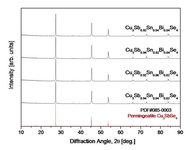
XRD patterns of Cu3Sb1-x-ySnxBiySe4 permingeatite synthesized via mechanical alloying and hot pressing.
Fig 2 presents the fractured surfaces of sintered Cu3Sb1-x-ySnxBiySe4. It was observed that the Sn and Bi contents did not affect the microstructure. In addition, no unreacted residual elements or secondary phases were observed. The right column in the SEM images shows the EDS elemental maps of Cu3Sb0.92Sn0.06Bi0.02Se4, which indicate that each element was homogeneously distributed. The relative density of the Sn/Bi double-doped permingeatite was 97.7%–98.2% (Table 1); the actual and nominal compositions did not differ significantly, and they were within the measurement error range. Therefore, a single permingeatite phase double-doped with Sn and Bi was successfully synthesized via MA and HP.
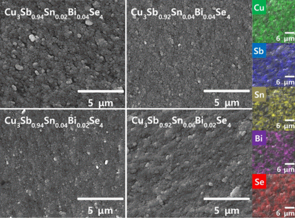
SEM images of fractured surfaces for Cu3Sb1-x-ySnxBiySe4 and EDS elemental maps of Cu3Sb0.92Sn0.06Bi0.02Se4.
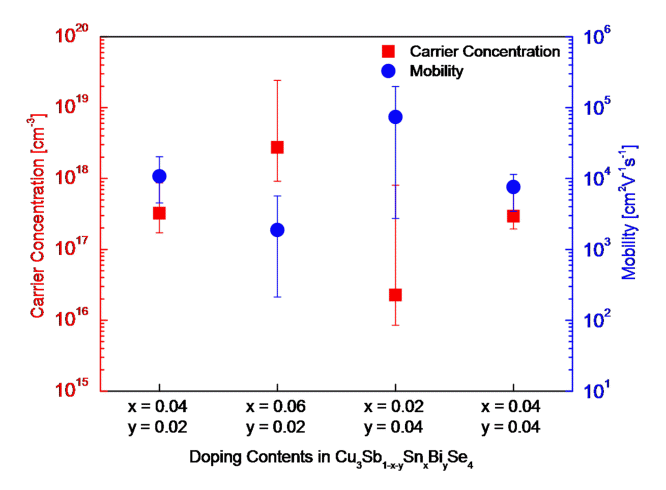
The charge transport characteristics of Cu3Sb1-x-ySnxBiySe4 are shown in Fig 3. The Hall coefficient values were positive, confirming that the majority charge carrier was holes in the p-type semiconductor. When the Bi content (y) was constant, the carrier concentration increased with the Sn content (x), i.e., from 3.24 × 10¹⁷ to 2.75 × 1018 cm-3 when y = 0.02, and from 2.28 × 10¹⁶ to 2.93 × 1017 cm-3 when y = 0.04. This was due to the additional holes generated by doping Sn4+ at the Sb5+ site. When the Sn content was constant, the change in the carrier concentration was insignificant, based on the Bi content. This was attributed to the valences of Bi5+ and Sb5+. Wei et al. [5] reported that Sn doping increased the carrier concentration of Cu2.95Sb1-xSnxSe4 (x = 0.00-0.04) from 5.02 × 10¹⁹ to 2.08 × 1020cm-3. Li et al. [18] achieved an increased carrier concentration in Cu3Sb1-yBiySe4 (y = 0.00-0.03), i.e., from 3.38 × 10¹⁸ to 7.21 × 1018 cm-3; however, it decreased to 2.89 × 1018 cm-3 when y = 0.03 owing to the presence of impurity phases.
In this study, when the Bi content was constant, the mobility decreased significantly as the Sn content increased, i.e., from 1.07 × 10⁴ to 1.88 × 103 cm2V-1s-1 when y = 0.02 and from 7.39 × 10⁴ to 7.59 × 103 cm2V-1s-1 when y = 0.04. However, when the Sn content was constant, the mobility slightly decreased from 1.07 × 10⁴ to 7.59 × 103 cm2V-1s-1 depending on the Bi content. Wei et al. [5] reported that as the Sn content increased in Cu3Sb1-xSnxSe4 (x = 0.01-0.04), the mobility decreased from 49 to 26 cm2V-1s-1. Li et al. [18] reported that as the Bi content increased in Cu3Sb1-yBiySe4 (y = 0.01-0.03), the mobility decreased from 1.65 × 10² to 1.06 × 102 cm2V-1s-1.
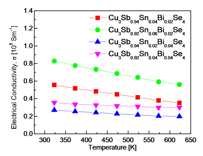
Fig 4 shows the electrical conductivity of Cu3Sb1-x-ySnxBiySe4. The electrical conductivity of a degenerate semiconductor is defined as σ = enμ (where e, n and μ are the electronic charge, the carrier concentration and the mobility, respectively) [19]. Therefore, electrical conductivity is affected by the temperature dependence of the carrier concentration and mobility. When the Bi content (y) was constant, the electrical conductivity increased with the Sn content (x), because of the increase in carrier concentration. In the temperature range of 323-623 K, the electrical conductivity increased from (5.56-3.51) × 104 to (8.28-5.61) × 104 Sm-1 for x = 0.04-0.06 when y = 0.02, whereas it increased from (2.69-1.97) × 104 to (3.56-3.00) × 104 Sm-1 for x = 0.02-0.04 when y = 0.04. However, when the Sn content was constant, the electrical conductivity decreased slightly as the Bi content increased, due to changes in the carrier concentration and mobility, as shown in Fig 3. Consequently, Cu3Sb0.92Sn0.06Bi0.02Se4 exhibited the highest electrical conductivity, whereas Cu3Sb0.94Sn0.02Bi0.04Se4 exhibited the lowest electrical conductivity.
Lee et al. [20] reported that the minimum electrical conductivity of Cu3SbSe4 was (4.23-4.88) × 103 Sm-1 at 323-623 K, which indicated nondegenerate semiconductor behavior. Compared with the undoped permingeatite, the electrical conductivity of permingeatite double-doped with Sn/Bi improved significantly in this study. Wei et al. [5] reported that electrical conductivity increased with Sn content in Cu3Sb1-xSnxSe4 (x = 0.01-0.04), where the highest electrical conductivity was 4.76 × 10³ Sm-1 at 673 K for Cu3Sb0.96Sn0.04Se4. Li et al. [18] obtained the highest electrical conductivity of 1.11 × 10⁴ Sm-1 at 600 K for Cu3Sb0.98Bi0.02Se4, among Cu3Sb1-yBiySe4 (y = 0.01-0.03). Liu et al. [13] investigated double-doped Cu3Sb1-x-ySnxBiySe4 (x = 0.02-0.10 and y = 0.02) and obtained the highest electrical conductivity of 7.85 × 10⁴ Sm-1 at 673 K for Cu3Sb0.88Sn0.10Bi0.02Se4.
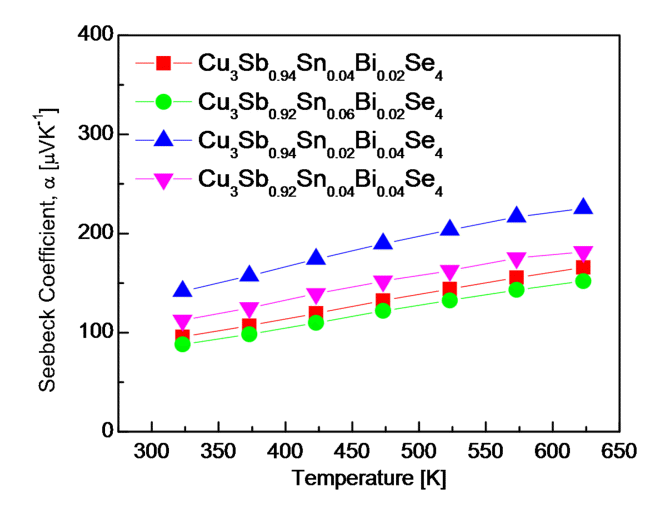
Fig 5 shows the Seebeck coefficients of Cu3Sb1-x-ySnxBiySe4. The permingeatite double-doped with Sn/Bi was a p-type semiconductor, which was reconfirmed from the positive Seebeck coefficient. The Seebeck coefficient is defined as a = (8/3)(π/3n)2/3(πkB/h)2m*Te-1 (where kB, h and m* are the Boltzmann constant, the Planck constant and the effective carrier mass, respectively) [21]. Because the Seebeck coefficient is inversely proportional to carrier concentration, it exhibits an opposite trend to the electrical conductivity. At a constant temperature, when the Bi content was constant, the Seebeck coefficient decreased with increasing Sn content, whereas when the Sn content was constant, the Seebeck coefficient increased with Bi content. Consequently, Cu3Sb0.94Sn0.02Bi0.04Se4 exhibited a maximum Seebeck coefficient of 141-225 μVK-1 at 323-623 K. Lee et al. [20] reported a Seebeck coefficient of 312-330 μVK-1 at 323-623 K for undoped Cu3SbSe4. Wei et al. [5] obtained a lower Seebeck coefficient by doping Sn into Cu2.95Sb1-xSnxSe4 (x = 0.01-0.04); they obtained a maximum Seebeck coefficient of 163-249 μVK-1 at 300-673 K for Cu3Sb0.99Sn0.01Se4. Li et al. [18] discovered that an intrinsic transition occurred at temperatures above 400 K for Cu3Sb1-xBixSe4 (x = 0.01-0.03), which resulted in a maximum Seebeck coefficient of 417 μVK-1 at 400 K for Cu3Sb0.98Bi0.02Se4. Liu et al. [13] reported that the double doping of Sn and Bi effectively increased the Seebeck coefficient of Cu3Sb1-x-ySnxBiySe4 (x = 0.02-0.10 and y = 0.02), and that Cu3Sb0.96Sn0.02Bi0.02Se4 achieved a maximum Seebeck coefficient of 149-279 μVK-1 at 323-673 K.
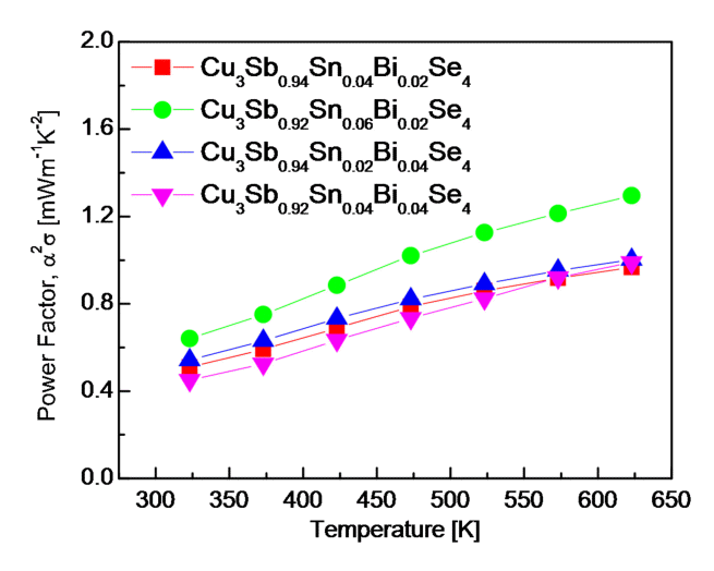
Fig 6 shows the PF of Cu3Sb1-x-ySnxBiySe4. The PF depends on the electrical conductivity and Seebeck coefficient, and these two parameters are affected oppositely by the carrier concentration [22]. The PF increased with temperature because the effect of increasing the Seebeck coefficient was greater than that of decreasing electrical conductivity caused by an increase in temperature. At a constant temperature, however, the increase in electrical conductivity by Sn/Bi double doping was more effective at increasing the PF than the decrease in the Seebeck coefficient. Consequently, Cu3Sb0.92Sn0.06Bi0.02Se4 achieved the highest PF of 0.64-1.29 mWm-1K-2 at 323-623 K. Compared with the PF of undoped Cu3SbSe4 (0.38-0.50 mWm-1K-2 at 323-623 K) [20], Cu3SbSe4 double-doped with Sn/Bi significantly increased the PF of permingeatite. Wei et al. [5] obtained a PF of 0.65-1.38 mWm-1K-2 at 300-673 K for Cu3Sb0.97Sn0.03Se4. Li et al. [18] reported that the PF decreased with temperature from 1.8 mWm-1K-2 at 323 K to 1.1 mWm-1K-2 at 600 K for Cu3Sb0.98Bi0.02Se4. In fact, Liu et al. [13] further increased the Seebeck coefficient by performing Sn/Bi double doping (as compared with only Sn doping) and achieved the highest PF of 1.81 mWm-1K-2 at 654 K for Cu3Sb0.88Sn0.1Bi0.02Se4.
The thermal conductivities of Cu3Sb1-x-ySnxBiySe4 are shown in Fig 7. After determining the electronic thermal conductivity (κE) using the Wiedemann–Franz law (κE = LσT), the lattice thermal conductivity (κL) was calculated from the measured thermal conductivity (κ) using the relation κ = κE+ κL [23,24], where the temperature-dependent Lorenz number (L) was estimated using the equation L = 1.5+ exp(– α ⁄ 116) [25, 26]. In this study, a specific heat of 0.32 Jg-1K-1 was used to evaluate the thermal conductivity [27], and Fig 7(a) shows the thermal conductivity of Cu3Sb1-x-ySnxBiySe4. The thermal conductivity decreased with temperature, and bipolar conduction did not occur within the measurement temperature range. At a constant temperature, the thermal conductivity decreased at higher Bi and lower Sn contents. However, a lower thermal conductivity was obtained at 523 K as the Bi content increased when the Sn content was constant at x = 0.04. Additionally, higher thermal conductivity was observed at temperatures above 523 K. This crossover in the thermal conductivity was similarly reported in Bi-doped permingeatite by Li et al. [18]. In this study, the lowest thermal conductivity of 1.40-0.91 Wm-1K-1 was obtained at 323-623 K in Cu3Sb0.94Sn0.02Bi0.04Se4. Wei et al. [5] reported a minimum thermal conductivity of 3.19-1.21 Wm-1K-1 at 275-700 K for Cu2.95Sb0.99Sn0.01Se4. Li et al. [18] obtained a minimum thermal conductivity of 1.97-0.98 Wm-1K-1 at 323-573 K for Cu3Sb0.98Bi0.02Se4. Liu et al. [13] reported the lowest thermal conductivity of 1.20-0.94 Wm-1K-1 at 323-673 K in Cu3Sb0.96Sn0.02Bi0.02Se4.

Temperature dependence of thermal conductivities of Cu3Sb1-x-ySnxBiySe4: (a) Total thermal conductivity and (b) electronic and lattice thermal conductivities.
Fig 7(b) shows the separate contributions to thermal conductivity. κE was attributed to the charge carriers, and κL was due to phonons. κE did not indicate a significant temperature dependence; however, it was directly affected by the carrier concentration, i.e., the Sn/Bi doping concentration. κE decreased because of the reduced carrier concentration as the Bi content increased and the Sn content decreased. Hence, a minimum κE of 0.15-0.19 Wm-1K-1 was achieved at 323-623 K in Cu3Sb0.94Sn0.02Bi0.04Se4.
The κE values achieved in other studies were as follows: 0.18-0.17 Wm-1K-1 at 275-700 K for Cu3Sb0.9Sn0.1Se4 [5], 0.05-0.11 Wm-1K-1 at 323-575 K for Cu3Sb0.7Bi0.3Se4 [18], and 0.15-0.22 Wm-1K-1 at 323-673 K for Cu3Sb0.96Sn0.02Bi0.02Se4 [13]. In this study, κL decreased as the temperature increased. When the Bi content was constant at 0.02, κL was lower as the Sn content increased; consequently, the lowest κL of 1.10-0.44 Wm-1K-1 was obtained at 323-623 K in Cu3Sb0.92Sn0.06Bi0.02Se4. However, when the Bi content increased to 0.04, κL increased as the Sn content increased. Therefore, when the Bi doping level was low, the addition of Sn effectively reduced κL, whereas when the Sn doping level was low, the addition of Bi effectively reduced κE. Wei et al. [5] reported that the κL of all samples of Cu2.95Sb1-xSnxSe4 (x = 0.01-0.04) was 2.81-1.01 Wm-1K-1 at 275-700 K. Li et al. [18] obtained a minimum κL of 1.87-0.79Wm-1K-1 at 323-573 K for Cu3Sb0.97Bi0.03Se4. Liu et al. [13] achieved the lowest κL of 0.89-0.27 Wm-1K-1 at 323-673 K for Cu3Sb0.88Sn0.1Bi0.02Se4.
Fig 8 shows the L of Cu3Sb1-x-ySnxBiySe4. Theoretically, the range of L is (1.45-2.44) × 10-8 V2K-2; higher numbers indicate degenerate semiconductor or metallic behavior, whereas smaller numbers indicate nondegenerate semiconductor behavior [21, 28]. A maximum L of (1.96-1.76) × 10-8 V2K-2 was obtained at 323-623 K in Cu3Sb0.92Sn0.06Bi0.02Se4, whereas a minimum L of (1.79-1.64) × 10-8 V2K-2 was achieved at 323-623 K in Cu3Sb0.94Sn0.02Bi0.04Se4. Sn doping increased L (shifted to the degenerate state); conversely, Bi doping decreased L (shifted to the nondegenerate state). Lee et al. [20] reported a L of (1.54-1.56) × 10-8 V2K-2 at 323-623 K for undoped Cu3SbSe4.
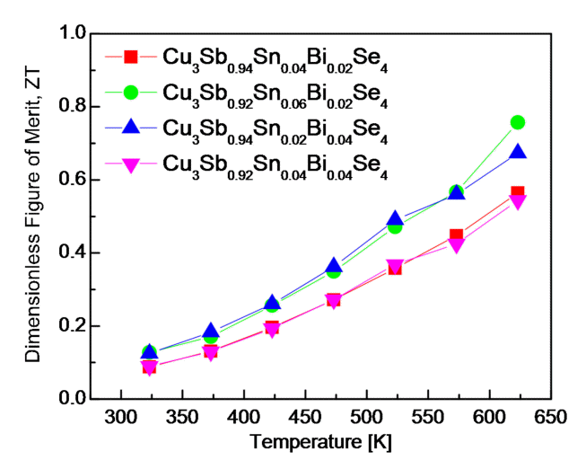
Fig 9 presents the ZT of Cu3Sb1-x-ySnxBiySe4. The highest ZT of 0.75 was obtained at 623 K in Cu3Sb0.92Sn0.06Bi0.02Se4, the result of its high PF and low thermal conductivity. Although the thermal conductivity was the lowest when x = 0.02 and y = 0.04, the maximum ZT value was attributed to the highest PF, when x = 0.06 and y = 0.02. Lee et al. [20] reported a ZT of 0.39 at 623 K for undoped Cu3SbSe4, which was synthesized via the same process as ours; the reported ZT value was approximately two times higher than that achieved via Sn/Bi double doping. Wei et al. [5] reported a ZT of 0.70 at 673 K for Cu3Sb0.98Sn0.02Se4 synthesized via MA and spark plasma sintering (SPS). Li et al. [18] obtained a ZT of 0.70 at 600 K for Cu3Sb0.98Bi0.02Se4 synthesized via melting–SPS. Liu et al. [13] achieved an extremely high ZT of 1.26 at 673 K for Cu3Sb0.88Sn0.10Bi0.02Se4 prepared via a multistep solution-based synthesis followed by HP; the thermal conductivity was approximately 1 Wm-1K-1, which was similar to our result, but the PF was 1.81 mWm-1K-2 (an anomalously high value for permingeatite), which was 1.4 times higher than ours (1.29 mWm-1K-2). These values were obtained because the carrier concentration was 1020cm-3, which was two orders higher compared with that of our specimen. In addition to the doping level, the measured temperature of the thermoelectric properties was higher than 623 K, which contributed to the high ZT value because it was proportional to the measured temperature below the temperature at which the intrinsic transition and bipolar conduction occurred.
4. CONCLUSIONS
Permingeatite Cu3Sb1-x-ySnxBiySe4 (x = 0.02–0.06, y = 0.02–0.04) double-doped with Sn and Bi at the Sb site was synthesized via MA–HP. XRD analysis revealed that both the synthetic powders and sintered specimens investigated in this study were composed of a tetragonal permingeatite phase without secondary phases. All elements in the sintered samples were distributed uniformly, with a relative density of 97.7%–98.2%. After Sn and Bi were substituted at the Sb site, the lattice constant changed to 0.56510-0.56518 nm for the a-axis and 1.12509-1.12529 nm for the c-axis. The Hall and Seebeck coefficients were positive, thereby confirming that the Sn/Bi double-doped permingeatite is a p-type semiconductor. Sn doping resulted in charge compensation due to additional electrons; hence, the carrier concentration increased from 2.27 × 10¹⁶ to 2.74 × 1018 cm-3, whereas the mobility decreased from 7.39 × 10⁴ to 1.88 × 103 cm2Vs-1. However, Bi doping did not significantly affect the charge transport properties. As the Sn content increased and the Bi content decreased, the electrical conductivity increased, where the highest electrical conductivity of (8.28-5.61) × 104 Sm-1 was exhibited at 323-623 K in Cu3Sb0.92Sn0.06Bi0.02Se4. In contrast, as the Sn content decreased and the Bi content increased, the Seebeck coefficient increased, resulting in the highest Seebeck coefficient of 141-225 μVK-1 at 323-623 K in Cu3Sb0.94Sn0.02Bi0.04Se4. Consequently, Cu3Sb0.92Sn0.06Bi0.02Se4 exhibited a maximum PF of (0.64-1.29) mWm-1K-2 at 323-623 K. Sn doping decreased the lattice thermal conductivity, whereas Bi doping reduced the electronic thermal conductivity but did not effectively reduce the lattice thermal conductivity. The lowest thermal conductivity of 1.40-0.91 Wm-1K-1 was obtained at 323-623 K in Cu3Sb0.94Sn0.02Bi0.04Se4. Consequently, a maximum ZT of 0.75 was achieved at 623 K by Cu3Sb0.92Sn0.06Bi0.02Se4.
Acknowledgements
This study was supported by the Basic Science Research Capacity Enhancement Project (National Research Facilities and Equipment Center) through the Korea Basic Science Institute funded by the Ministry of Education (Grant No. 2019R1A6C1010047).

