


1. INTRODUCTION
A high-impedance surface is defined as a high voltage to low current surface, and is utilized as the grounded layer for quarter wavelength thick electromagnetic wave absorbers, such as Dallenbach layers [1] or Salisbury screens [2]. A resistive frequency selective surface (FSS) can also be efficiently employed on this high-impedance surface in order to design wideband absorbers [3-7]. The resonance frequency of the FSS, which can be controlled by its patterns or geometries, corresponds to the center frequency of the absorption band. By combining two or three arrays of FSSs with different patterns or geometries (thus with different resonance frequencies) in a multi-layer structure, a significant enlargement of the absorption bandwidth has been achieved [8-15].
A square loop conductive array has been the typically adopted pattern for FSS, because it has the advantages of both high inductance and high capacitance, and it has been used in the design of wide bandwidth absorbers in single- or multi-layer structures [3,8,14]. A low-pass array of square patches has been proposed as the capacitive circuit absorbers, with a large bandwidth and an optimal thickness [16,17]. Due to the high capacitance and low inductance, the square patch FSS has some benefits; the problems of anti-resonances and harmonics can be avoided, and spacers with flexible thicknesses (i.e. not fixed to the quarter wavelength) can be utilized. For the resistive square patch FSS, in addition, better control of dimension and surface resistance is possible during the screen printing process, due to its simple pattern and large surface area.
In this paper, a reliable and efficient numerical method is presented for the design of broadband absorbers, by layering two square patch-frequency selective surfaces (SP-FSS) with different geometries on a grounded dielectric substrate. The circuit parameters of inductance and capacitance of the SP-FSS are retrieved using the strip wire conductor model [18]. The optimal design for the surface resistance and layer thickness of the double-layer absorber provided a 10 dB absorption bandwidth of 6.1−41.4 GHz. The total thickness of the absorber was 5 mm, which is equal to the theoretical limit, demonstrating the novelty of the proposed design method and optimization. The free space measurement with a prototype prepared by the screen printing method also demonstrated a wide-bandwidth absorption result (4.7−40.0 GHz for −10 dB reflection loss) and quite thin total thickness (5.4 mm), which verified the numerical prediction for the wide bandwidth SP-FSS absorbers.
2. INDUCTANCE AND CAPACITANCE OF SP-FSS
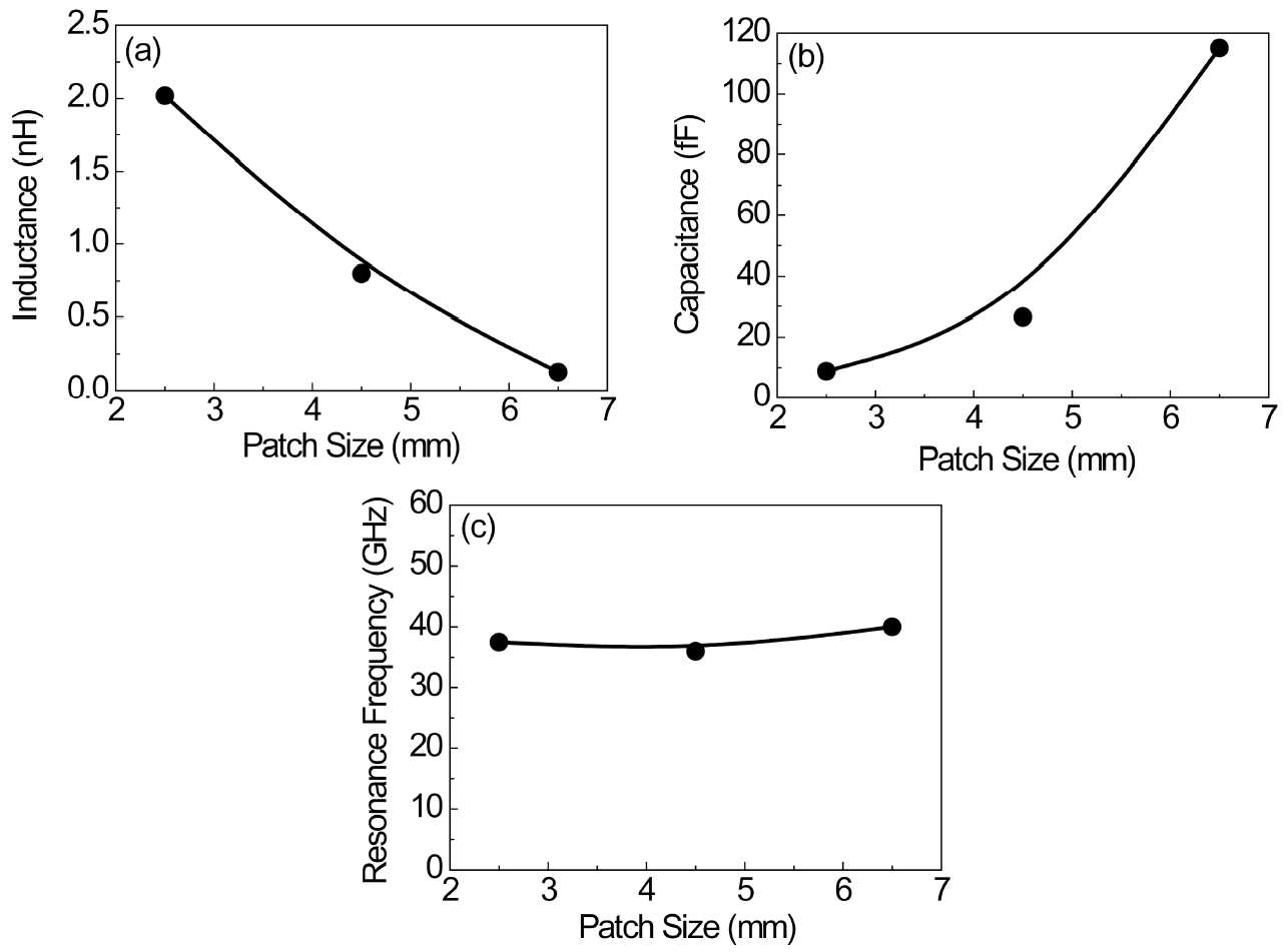
Fig 1 illustrates the SP-FSS standing in free space, its dimensions, and its equivalent circuit. The dimensions of the unit cell period (p), SP-FSS length (d), and interval space (g) between the two SP-FSSs are given in Fig 1(b), and patch size is varied (d = 2.5~6.5 mm) at a constant cell periodicity (p = 7.5 mm). The equivalent circuit can be represented as a shunted L-C series circuit across the transmission line (Fig 1(c)).
A computational tool (ANSYS HFSS 13.0) was used to determine the transmission loss for the SP-FSS structures. The simulation result is presented in Fig 2, showing a single principal resonance at a frequency (f0) of 36 GHz for SP-FSS with the dimensions p = 7.5 mm, d = 4.5 mm, and g = 3.0 mm.
The inductance (L) and capacitance (C) of the SP-FSS can be calculated using the equations for a flat wire conductor with width (w), thickness (tc), length (l), and gap (g) between the two SP-FSSs, which are given by [18]:
Fig 3 shows the variation in the circuit parameters (L, C) and resonance frequency of the SP-FSS with increasing patch sizes, from d = 2.5 mm to d = 6.5 mm at a constant unit cell periodicity p = 7.5 mm. By increasing the patch size, the L decreases, but the C increases, resulting in a nearly constant resonance frequency given by f0 = 1/[2π(LC)1/2] ≈ 37 GHz.
3. SINGLE-LAYER ABSORBER DESIGN
For a single-layer microwave absorber composed of an SP-FSS on the top layer and a ground conductor on the bottom layer, the complex admittance of the SP-FSS (YFSS) and the grounded substrate (Yt) are expressed as follows:
where Y0 isthe free space admittance (= 1/377 Ω-1); ω is the angular frequency; εr and μr are the relative permittivity and permeability of the substrate, respectively; t is the thickness of the substrate; c is the velocity of light.
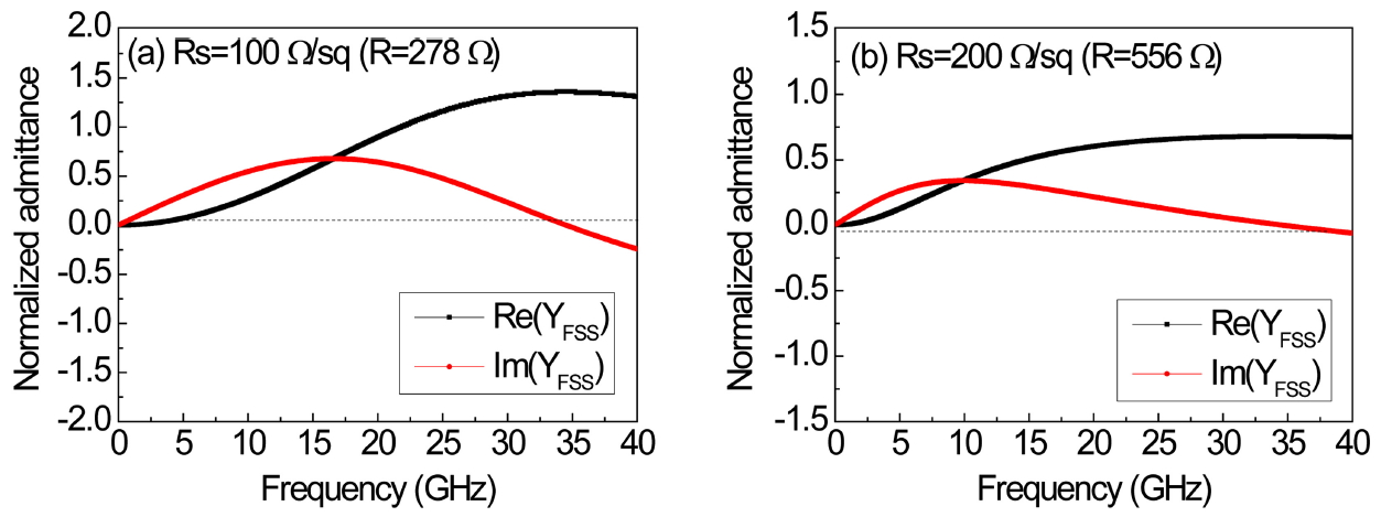
Fig 4 presents the normalized admittance of the SP-FSS (YFSS/Y0 = Re(YFSS) + jIm(YFSS)) with the dimensions p = 7.5 mm, d = 4.5 mm, and g = 3.0 mm. The previously determined L (= 0.8 nH) and C (= 26.5 fF) values were used, assuming the substrate to be air. The FSS resistance (R) can be calculated from the surface resistance of the conductor (Rs): R = Rs(B/A), where A is the patch size (= d × d) and B is the unit cell area (= p × p). The resonance frequency is at the high frequency of around 35 GHz, where Im(YFSS) = 0. Below the resonance frequency, the circuit is capacitive (Im(YFSS) ≥ 0), due to the large value of C of the SP-FSS. The real part Re(YFSS) exhibits a broad frequency dispersion due to the Ohmic loss of the SP-FSS. At an appropriate surface resistance of the SP-FSS, the real part approaches to the free-space admittance (Re(YFSS) = 1). For an SP-FSS with Rs = 100 Ω/sq (R = 278 Ω), Re(YFSS) ≈ 1 at frequencies above 25 GHz (Fig 4(a)). With a higher surface resistance (Rs = 200 Ω/sq), Re(YFSS) ≤ 1 for all frequencies (Fig 4(b)).
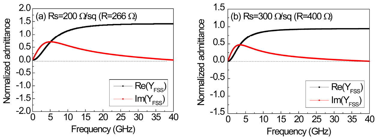
A similar behavior of complex admittance was predicted for a larger SP-FSS, as shown in Fig 5. With a bigger patch size (d = 6.5 mm), the equivalent circuit is capacitive (Im(YFSS) ≥ 0) below a resonance frequency. The real part has the freespace admittance (Re(YFSS) ≈ 1) at a higher surface resistance (Rs = 300 Ω/sq), due to the bigger patch size (Fig 5(b)).
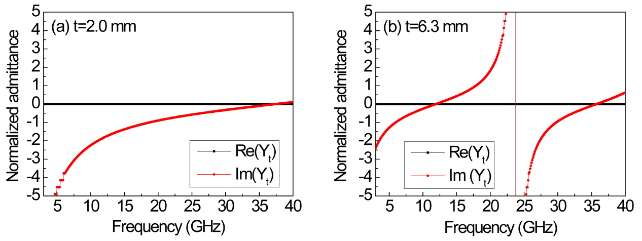
The normalized input admittance of a grounded substrate (Yt/Y0= Re(Yt) + jIm(Yt)) with varying thickness (t = 2.0~6.3 mm) is illustrated in Fig 6. A short-circuit resonance is found at the frequency where Im(Yt) = 0, and there the spacer thickness is equal to a quarter wavelength. For a small spacer thickness (t = 2.0 mm), the circuit is inductive for all frequencies below 37 GHz, as shown in Fig 6(a). The inductive grounded substrate of a small thickness exhibits the inverse frequency dispersion against the capacitive circuit characteristic of SP-FSS presented in Fig 4 and Fig 5. For a large spacer thickness (t = 6.3 mm), the resonance is found at two frequencies (12.5 GHz and 37.0 GHz), as shown in Fig 6(b). The first resonance results from the high-impedance surface of the one quarter wavelength thickness, and the second resonance corresponds to the high-impedance surface of the three quarter wavelength thickness. Due to the zero dielectric loss of the substrate (air), Re(Yt) is zero for all frequencies.
Fig 7 depicts the normalized total admittance (YTotal/Y0 = Re(YTotal) + jIm(YTotal)) of the grounded substrate with the SP-FSS on the top surface, which is a parallel circuit of the complex admittance of the SP-FSS (YFSS) and the input admittance of the grounded substrate (Yt). This is expressed as follows:
Perfect absorption can be obtained at the admittance matching condition, which is given by Re(YTotal) = 1 and Im (YTotal) = 0.
The parallel circuit combination of the input admittance of the grounded substrate and the complex admittance of the SP-FSS can lead to admittance matching in a broad frequency range. For an SP-FSS with dimensions p = 7.5 mm, d = 4.5 mm, and g = 3.0 mm and Rs = 100 Ω/sq (hereafter designated SP-FSS1) placed on a grounded air spacer with t = 2 mm, Im(YTotal) ≈ 0 in a broad frequency range above 25 GHz and Re(YTotal) ≈ 1, as depicted in Fig 7(a). For the SP-FSS with p = 7.5 mm, d = 6.5 mm, and Rs = 300 Ω/sq (designated SP-FSS2) placed on a thicker grounded air substrate (t = 5 mm), the admittance matching condition (Re(YTotal) ≈ 1 and Im (YTotal) ≈ 0) is satisfied at two frequencies (13 GHz and 45 GHz), as depicted in Fig 7(b), which produces the dual-band absorber.
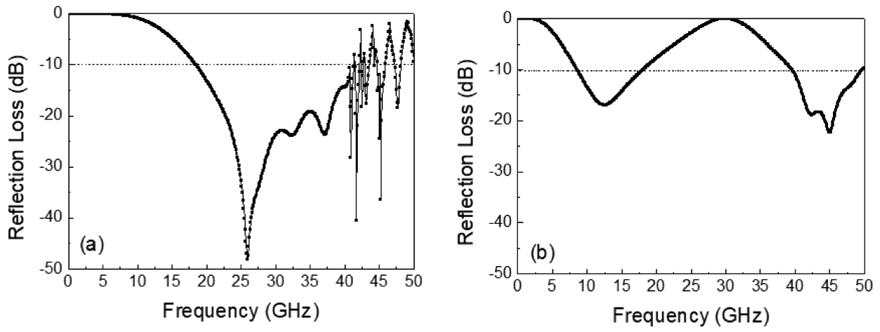
Fig 8 presents the reflection loss for the SP-FSS1 and SP-FSS2 absorbers designed with an optimized admittance matching combination of SP-FSS and substrate. For SP-FSS1 (Rs= 100 Ω/sq) on air substrate (t = 2 mm), a broad bandwidth is predicted with a reflection loss lower than −10 dB in the frequency range above 17.5 GHz, as depicted in Fig 8(a). For SP-FSS2 (Rs= 300 Ω/sq) on air substrate (t = 5 mm), a dual-band absorption is predicted with a reflection loss lower than –10 dB at two matching frequencies of 13 GHz and 45 GHz (Fig 8(b)).
4. DOUBLE-LAYER SL-FSS ABSORBER DESIGN
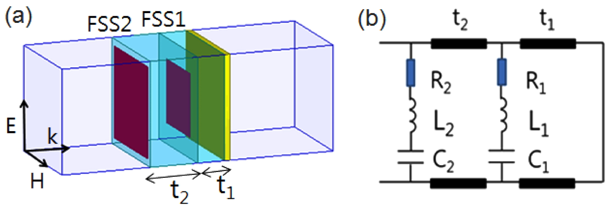
A planar electromagnetic absorber consisting of two resistive SP-FSS layers was designed and is illustrated in Fig 9(a), and the equivalent circuit is presented in Fig 9(b). For the double-layer SP-FSS absorber, SP-FSS1 was placed on a grounded substrate with a thickness of t1 and SP-FSS2 was placed on the second substrate with a thickness of t2. The two resistive SP-FSSs are characterized by their resistance (R1, R2), inductance (L1, L2), and capacitance (C1, C2).
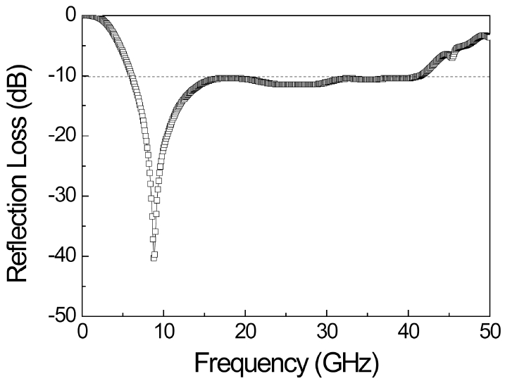
The ultrawide bandwidth of the double-layer SP-FSS absorber is presented in Fig 10. The design parameters are the R, L, and C of each SP-FSS and the substrate thickness (t1, t2). The optimized circuit parameters and layer thickness are given in Table 1. The reflection loss decreased to less than –10 dB in the broad frequency range of 6.1–41.4 GHz.
where Γ is the reflection loss in dB and λ is the wavelength. Using the absorption bandwidth (6.1–41.4 GHz for Γ = –10 dB), the theoretical limit of the total thickness is estimated to be t = 5.0 mm. The total thickness of the present work is 5.0 mm, equal to the theoretical limit, demonstrating the novelty of the proposed design method and optimization.
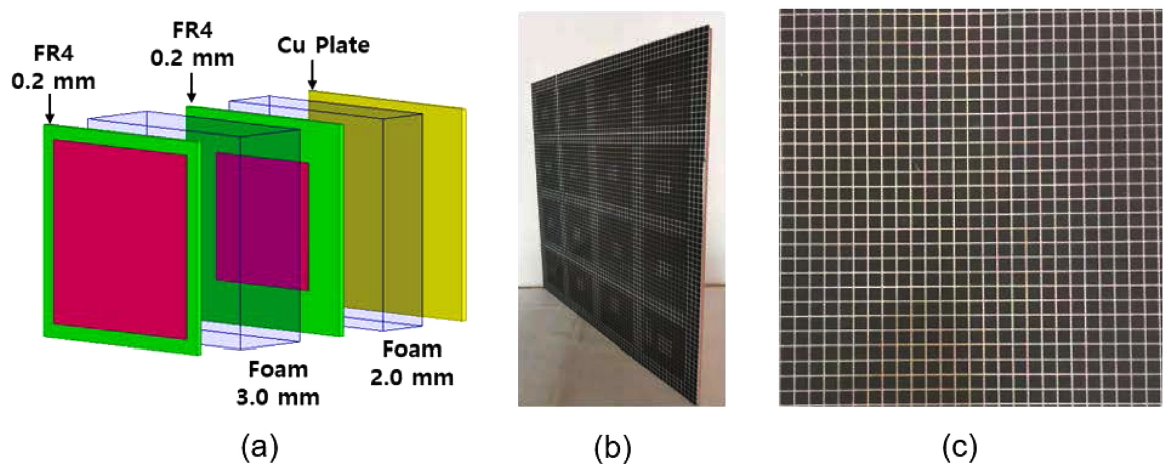
The SP-FSS were fabricated with an optimum design using a screen printing method, which has been described in detail in previous works [11,14]. Using FR4 (with a permittivity of εr= 4.05 + j0.017 and 0.2 mm thickness) as the printing substrates, and polyethylene foam (εr= 1.05 + j0.02) as the space material, a two-layer absorber was constructed with a terminal plate of Cu (Fig 11(a)). The thickness of the space material was t1= 2.0 mm and t2= 3.0 mm. The total thickness was 5.4 mm, including the FR4 substrates. The prototype test sample was 50 cm × 50 cm in size including 66 × 66 unit cells arrays (Fig 11(b)). The screen-printed pattern of the SP-FSS (p = 7.5 mm, d = 6.5 mm) is shown in Fig 11(c).
Measurements were carried out in an anechoic chamber using an Agilent vector network analyzer and two horn antennas for four different frequency bands (1−18 GHz, 18−30 GHz, 26.5−40 GHz, 40−50 GHz). After the reflection coefficient was normalized, using the backed metallic plate of the structure acting as an ideal reflector, measurements of power reflection were made for the test samples.
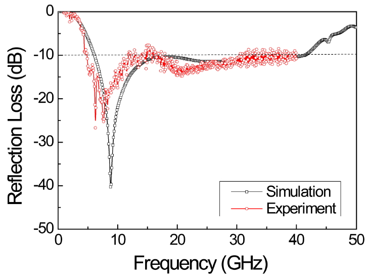
Fig 12 presents the experimental results of the reflection loss for normal incidence of a TEM wave, depicting a 10 dB absorption bandwidth of 4.7−40.0 GHz. Compared with the simulation result, the absorption band was slightly shifted to lower frequencies. This was attributed to the insertion of high-permittivity materials (FR4) and a slight increase in spacer thickness. The total thickness was 5.4 mm, quite thin as low as 0.08λL (λL: wavelength at the lowest operation frequency), typical values of which are at the level of 0.11~0.15λL [8-11]. The experimental results strongly validated the proposed SP-FSS absorbers design.
5. CONCLUSION
A microwave absorber with wide bandwidth and theoretical value small thickness was demonstrated, utilizing SP-FSS with different geometries in a double-layer structure. The optimally designed surface resistance and layer thickness of the double-layer absorber provided a 10 dB absorption bandwidth of 6.1–41.4 GHz. The total thickness of the absorber was 5 mm, which is equal to the theoretical limit, demonstrating the novelty of the proposed design method and optimization. The free space measurement also demonstrated a wide-bandwidth absorption result (4.7-40.0 GHz for −10 dB reflection loss) and quite thin total thickness (5.4 mm), which was in good agreement with the simulation result. The experimental result also strongly validated the proposed design method for the wide-bandwidth SP-FSS absorbers. In addition, the SP-FSS provides better control of dimension and surface resistance during the screen printing process, leading to easy production of the ultrawide bandwidth absorbers.