


1. INTRODUCTION
Thermoelectric materials can convert temperature gradients into electrical potential and vice versa. A high thermoelectric conversion efficiency is required to utilize the potential created from waste heat generated in various industries and automobiles. The thermoelectric conversion efficiencies are evaluated using a dimensionless thermoelectric figure-of-merit, zT = S2ŽāT/╬║, where S, Žā, ╬║ and T are the Seebeck coefficient, the electrical conductivity, the total thermal conductivity and the absolute temperature, respectively. Accordingly, a high power factor S2Žā or low ╬║ is required for thermoelectric materials to achieve a high zT [1,2]. Conventional thermoelectric materials such as Bi2Te3 [3], PbTe [4] and CoSb3 [5] have been widely studied for decades in efforts to improve their thermoelectric performance. Nanostructuring [6], doping [7] and carrier filtering [8] have been considered effective approaches to enhance zT by either increasing the power factor or reducing ╬║. Meanwhile, other efforts have been focused on discovering new thermoelectric materials. Among the various new thermoelectric materials, post-transition metal chalcogenides such as SnSe [9], In4Se3 [10] and In2Se3 [11], which consist of a two-dimensional layered structure, have attracted significant attention due to their intrinsically low lattice thermal conductivity (╬║latt), which is caused by the weak atomic bonding between layers (van der Waals bonds). Additionally, SnSe and In4Se3 materials exhibit a special phenomenon in which lattice softening [9] of the charge density wave (CDW) [10] occurs as the temperature increases. This greatly reduces the lattice thermal conductivity, ╬║latt. Because of these properties, post-transition metal chalcogenides have been studied as potential thermoelectric materials.
The post transition metal indium selenide (InSe) is a III-VI group semiconductor with a band gap of ~1.2 eV. It exhibits a strong covalent bond within layers and a weak van der Waals bond between layers. Due to the weak van der Waals bond between the layers, the reported thermal conductivity of an InSe crystal in directions parallel and perpendicular to the c-axis was 0.37 and 1.2 W/mK, respectively [12,13]. These results suggest InSe-based alloys may be good candidates to achieve high zT by optimizing electrical properties such as carrier concentration, mobility and band structure. In previous studies, substitutes like Si, Sn and As have been suggested as shallow donors [14]. Lee et al. reported that Si acts as a shallow donor in InSe, to modify the electronic structure including the carrier concentration and mobility [15]. Anion doping of Se/Te in InSe also increased the carrier concentration [16]. Therefore, we suggested the possibility that group IV elements such as Ge and Sn could enhance the electrical properties of InSe.
In this study, we investigated the influence of Sn doping (a group IV element), which acted as a shallow donor in InSe, to enhance electrical properties. We synthesized a series of Sn-doped InSe (In1-xSnxSe, x = 0, 0.03, 0.05, 0.15 and 0.2) polycrystalline samples. Sn doping significantly increased the carrier concentration while reducing mobility only to a certain extent. As a result, the Žā largely increased while the S was moderately reduced, thus enhancing the power factor. Regardless of the increase in the Žā, ╬║ hardly changed with Sn doping due to the negligible electronic contribution in ╬║. As a result, the value of zT for the Sn-doped InSe sample increased to 0.14 as compared to a zT value of 0.04 for the pristine InSe.
2. EXPERIMENT
A series of In1-xSnxSe compositions with nominal x = 0, 0.03, 0.05, 0.15 and 0.2 were synthesized by a conventional solid-state reaction in a vacuum-sealed quartz tube with stoichiometric compositions. Stoichiometric amounts of In, Sn and Se powders (In: 99.995%, Sn: 99.995%, Se: 99.999%) were mixed and reacted in a fused vacuum quartz tube at 500 ┬░C for 48 h. The synthesized ingots were ground into powders using a mortar. The polycrystalline samples were compacted using spark plasma sintering (SPS) at 430 ┬░C for 5 min under 70 MPa.
The crystalline phases of the samples were identified using X-ray diffraction (XRD) with Cu K╬▒. The Žā and S were measured simultaneously using a thermoelectric property measurement system, ZEM-3, perpendicular to the pressing direction, as the temperature was increased from 300 to 800 K. The Hall measurement was performed in the van der Pauw configuration using a Hall measurement system, from room temperature to 500 K. The ╬║ was calculated using the relationship ╬║ = Žüs┬ĘCp┬Ę╬╗, where Žüs, Cp, and ╬╗ are the sample density, heat capacity, and thermal diffusivity, respectively. The ╬╗ was measured using a laser-flash method, perpendicular to the pressing direction, as the temperature was increased from 300 to 800 K. The theoretical density of each sample with nominal composition was used to calculate ╬║. Further, the value of Cp of InSe was considered to be 0.255 J/g┬ĘK for all the samples.
3. RESULTS AND DISCUSSION
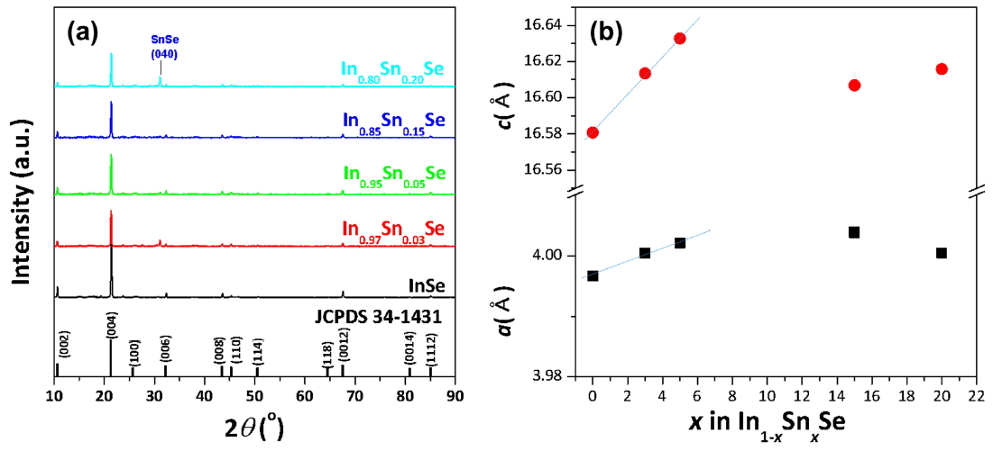
Figures 1(a) and 1(b) show the XRD patterns and the calculated lattice parameters for a series of Sn-doped InSe (In1-xSnxSe, x = 0, 0.03, 0.05, 0.15 and 0.2) polycrystalline samples. As seen in Figure 1(a), single-phase InSe samples were successfully synthesized. The SnSe impurity was observed rather intensively for In0.8Sn0.2Se. The lattice parameters, a and c, are as shown in Figure 1(b). The values of a and c increased continuously for x = 0, 0.03, and 0.05 because the ionic radius of In2+ (80 pm) was smaller than that of Sn2+ (93 pm). The continuous change in the lattice parameters indicated that substitutional doping of Sn at the In site was successful. Beyond x = 0.05, the second phase of SnSe precipitated and complete doping was not achieved; moreover, the lattice parameters changed rather irregularly. Therefore, the characterization was only performed for the small doping samples (x = 0, 0.03, and 0.05).
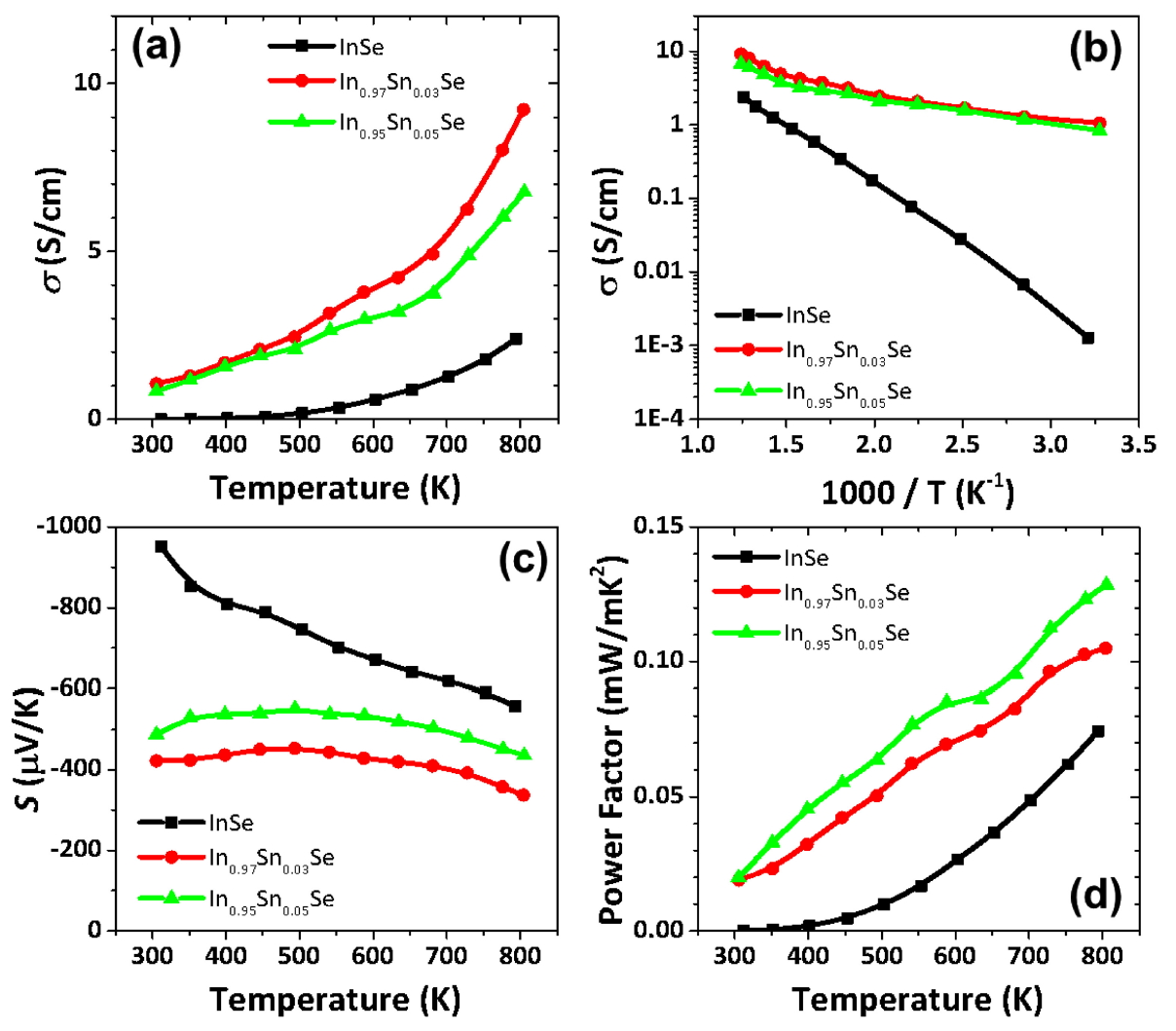
Figure 2(a) shows the Žā as a function of temperature for a series of Sn-doped InSe (In1-xSnxSe, x = 0, 0.03, 0.05) samples. It can be observed that the value of Žā increases as the temperature increases, which is a typical behavior of a non-degenerated semiconductor. The Žā values at room temperature were 0.001, 1.063 and 0.839 S/cm for x = 0, 0.03, and 0.05 in In1-xSnxSe, respectively, which generally increased with Sn doping. At 800 K, Žā increased to a maximum value of 9.221 S/cm for x = 0.03. Figure 2(b) shows the logarithm of Žā as a function of 1000/T, which indicates that the transport mechanism is changing around 660 K (where 1000/T is ~ 1.5). The activation energy (Ea) for Žā as a function of temperature based on the Arrhenius`s relationship (Žā ŌłØ exp (ŌłÆEa/kT), where k and T are the Boltzmann constant and absolute temperature, respectively) changes around 660 K. When InSe is doped with Sn, Ea decreases as seen in Figure 2(b), which means that the ratio of increase in Žā to the increase in temperature is higher at all temperatures for the Sn-doped sample, as compared to that of the pristine InSe.
Figure 2(c) and (d) show the S and the power factor as a function of temperature for a series of Sn-doped InSe (In1-xSnxSe, x = 0, 0.03, 0.05) samples. Due to the inverse relationship between Žā and S, the value of S for pristine InSe (ŌłÆ952.5 ╬╝V/K) when doped with Sn decreased to ŌłÆ422.6 and ŌłÆ488.1 ╬╝V/K for x = 0.03 and 0.05 at room temperature, respectively. The power factor increased when doped with Sn due to an increase in Žā; at 800 K, a maximum value of 0.13 mW/mK2 at x = 0.05 in In1-xSnxSe was observed.
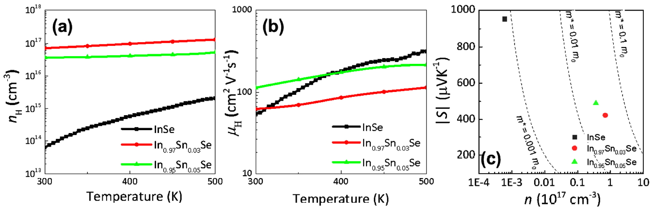
The carrier concentration and mobility of a series of Sndoped InSe (In1-xSnxSe, x = 0, 0.03, 0.05) samples are depicted in Figure 3(a) and (b). The carrier concentration significantly increased from 0.0021 ├Ś 1016 for x = 0 to 7.12 ├Ś 1016 for x = 0.03 and 3.69 ├Ś 1016 for x=0.05 at 300 K. Since the Sn impurity acted as a shallow donor in InSe, the carrier concentration could be extensively generated [14]. On the other hand, the mobility changed slightly, such that it increased at low temperatures and decreased at high temperatures.
Figure 3(c) shows the values of S as a function of the electron concentration (Pisarenko plot) at 300 K for the Sndoped samples. The dotted curves are plotted for effective mass (m*, expressed with respect to mo) of 0.001, 0.01 and 0.1 using the Mott-relation [17], expressed by Equation (1):
where e, h, and n are the elementary charge, the Planck constant, and the carrier concentration, respectively. When doped with Sn, the m* became more than 10 times higher than that of pristine InSe.
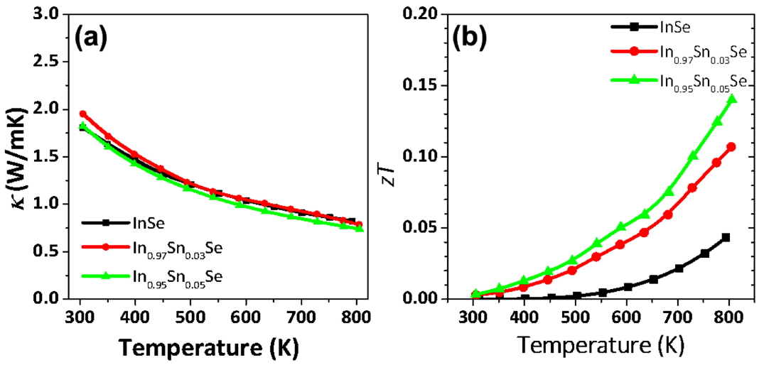
Figure 4(a) shows the values of ╬║ for a series of Sn-doped InSe (In1-xSnxSe, x = 0, 0.03, 0.05) samples, which did not change much with doping. At 300 K, the ╬║ values were 1.8, 1.9 and 1.8 W/mK for x = 0, 0.03 and 0.05, respectively. The increase in Žā would raise the electronic contribution, i.e., the electronic thermal conductivity (╬║elec), since ╬║elec is proportional to the Žā. However, the ╬║ was almost unchanged despite the Žā increase because ╬║elec was less than about 1% of ╬║.
Using the measured values of Žā, S, and k for the pristine InSe and the Sn-doped InSe samples, the value of zT was calculated and is shown in Figure 4(b). At 800 K, the zT values were 0.04 for pristine InSe and 0.11 and 0.14 for x = 0.03 and 0.05 samples, respectively. The zT values of the Sn-doped InSe samples increased compared to that of the pristine InSe. The enhancement in zT was attributed to the increase in Žā due to the significantly increased electron concentration. As a result, it was concluded that Sn substitution in InSe behaved as a shallow donor in InSe and enhanced electrical properties and the zT.
4. CONCLUSION
We measured the electrical and thermal transport properties of a series of Sn-doped InSe (In1-xSnxSe, x = 0, 0.03, 0.05) samples to explore the effects of Sn doping on InSe. The Sn doping significantly increased the carrier concentration and the electrical conductivity, as the substituted Sn acted as a shallow donor. Although the Seebeck coefficient decreased due to an inverse relationship with the carrier concentration, the power factor was effectively enhanced as a result of an increase in the effective mass of the Sn-doped samples. The thermal conductivity was unchanged because the electronic contribution to thermal conductivity was negligible. Consequently, the Sn doping in InSe enhanced the value of zT from 0.04 to 0.14 at 800 K when doped with Sn (at x = 0.05).