


1. INTRODUCTION
Zinc oxide (ZnO) is a typical n-type compound semiconductor with high transparency, a direct wide band gap (3.3 eV), a wide range resistivity (10-4 to 1012 Ω·cm), large free exciton binding energy (60 mV), and high electron Hall mobility (200 cm2Vs-1) at room temperature [1]. In parallel with multiple studies on pure ZnO, the research efforts to explore doping ZnO have been growing rapidly. Doped ZnO is applied to various applications such as magnetic memory devices, light emitting diodes, solar cell, transducer, surface-acoustic-wave device and chemical sensors [2-7]. Recently, ZnO has been actively studied in two aspects. It is the realization of the p-type semiconductor and the strengthening of the ferroelectricity. First, to develop a photoelectric material based on ZnO, p-type ZnO is required [8]. Li is representative among the additives used to realize these p-type semiconductors. Li doping has a high thermal diffusion, which improves crystal growth and improves c-axis orientation. In fact, it has been reported that it has produced p-type ZnO films using lithium [9,10]. Nevertheless, the increase in Li doping could lead to irregular crystal growth, which could lead to loss of crystal orientation. And, non-melted Li atom can be separated from the crystals and inhibited the growth of the crystals. [11]. These factors act as a hindrance to making p-type semiconductors. Second, when Li was added, it was reported that the ferroelectricity was strengthened. The substitution of Li ion smaller than the Zn ion radius prevents the center of the positive and the negative charge from overlapping, which appears to have induced a spontaneous divergence [12]. Therefore, theoretically and experimentally, the importance of dopants and their influences on optical, magnetic and electrical properties had been evaluated.
So far Li doped ZnO thin films have been manufactured in various ways, such as RF sputtering, pulsed-laser deposition, and so on [13-15]. Of these, sol-gel method has many advantages compared to other methods, such as producing large-area film coatings, relatively inexpensive cost, and giving easy control of film composition [16]. However, the sol-gel method has several drawbacks compared to others, such as high sintering temperature and the generation of other unexpected crystal phases as a result. In other words, the reaction at high sintering temperatures can develop a new crystal phases in the ZnO films. As such, investigators have reported the formation of Zn2SiO4 phases in ZnO film by the diffusion of the Si atoms on the silicon substrate [17,18]. Therefore, it is necessary to explore the formation of new crystal phase for Li-doped ZnO thin films on the silicon substrates. The authors used the XRD to scrutinize the change in crystal phases according to the different sintering temperatures. Also, the optical properties were measured by using cathodoluminescence (CL) in the wavelength region of 200 ~ 700 nm at room temperature.
2. EXPERIMENTAL PROCEDURES
Zn0.99Li0.01O films were deposited on silicon substrates by using the sol-gel method. As starting materials, zinc acetate dehydrate ((CH3CO2)2Zn·2H2O, Aldrich) and lithium acetate dehydrate ((CH3COO)2Li·2H2O, Aldrich) were used. The prepared materials were dissolved in methanol (CH3OH, Junsei Guaranteed Reagent) to make the precursor solution of Li doped ZnO about 0.4 M in concentration. A magnetic stirrer stirred the prepared solution for 48 h at room temperature. For washing the substrate, ultrasonic cleaning was performed using alcohol and distilled water, respectively. As a final step, the substrate was cleaned with nitrogen gas. The spin-coating was performed on pre-cleaned silicon substrates at spinning speed of 4500 and 5000 rpm, and were then dried about 120 °C for 3 min for gelation process in the air. The films were deposited at various sintering temperatures from 600 °C to 1000 °C at the heating rate of 200 °C/h in the air. The structural properties were investigated using X-ray diffraction (XRD). The surfaces of the samples were observed by using FE-SEM. CL measurements were performed at room temperature.
3. RESULTS AND DISCUSSION
Figure 1 shows the XRD patterns of the Zn0.99Li0.01O films deposited on Si substrates at various sintering temperatures from 600 °C to 1000 °C. As seen in Fig 1, the prominent peaks of the typical hexagonal phase of wurzite structure were observed from 2θ = 20o to 60°, and these peaks were indexed to be (100), (002), (101), (102), and (110) crystal planes, respectively. At sintering temperature of 600 °C and 700 °C (Fig (a)1, (b)1), there were no major changes in the wurizite structure of the samples. However, as the sintering temperature was increased above 800 °C (Fig 1(c)), new phases were emerged in the XRD patterns. At sintering temperature of 800 °C, a new diffraction peak appeared at 2θ = 22.06° on the XRD pattern as seen in Fig 1 (c). Although the diffraction peak at 2θ = 22.06° may be thought as the (101) diffraction of the willemite Zn2SiO4, we may not so. Because the typical Zn2SiO4 willemite own emission about 528 nm was not found in CL (Fig.4) [19,20]. Therefore, the peak (2θ = 22.06°) is considered to be the diffraction peak of the (101) plan in SiO2 cristobalite structure (21.984°, JCPDS No. 39-1425). At sintering temperature of 900 °C (Fig 1(d)), new peaks appeared at 24.4°, 31.52°, 44,4°, 48.84°, and 51.3°, respectively. It can be attributed to the (111), (200), (212), (214), and (100) planes of Li2SiO5 (JCPDS No. 42-0248), respectively. Moreover, more new peaks appeared at sintering temperature of 1000 °C (Fig 1(e)), such as 32.44°, 33.00°, and 33.96°. It may be due to the crystalline phase by the chemical bonding of silicon and lithium atoms, such as Li2SiO5, or Li8SiO6.
Fig 1 shows new phases appeared as sintering temperatures were increased. It is pointed out that the silicon atoms from the silicon substrate were diffused to thin films and chemically bound to doping material lithium.
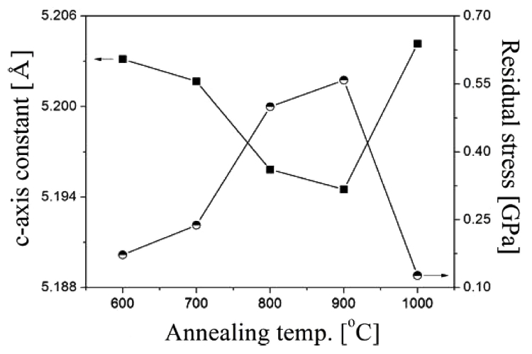
Figure 2 shows the changes of c-axis lattice constant and the stress in Zn0.99Li0.01O films sintered at various sintering temperatures. As the sintering temperatures are increased from 600 °C to 900 °C, the positions of the (002) peak in Fig 1 are shifted to a higher value of 2θ = 34.44°, 34.46°, 34.50°, and 34.51°, respectively. On the other hand, the position of the (100) peak is constant regardless of the sintering temperatures. The change in the (002) peak’s position means that c-axis lattice constant is changed and the films maintain uniform state of stress. The stress affects significantly the structure and properties of Li doped ZnO films to some extent. Therefore, it is important to reveal the stress of Li doped ZnO films. For Li doped ZnO films having wurtzite structure, the stress can be calculated from following formula. σ = 2 C 13 2 - C 33 ( C 11 + C 12 ) 2 C 13 · C + C 0 C 0 1 d 2 = 4 3 h 2 + hk + k 2 a 2 + l 2 c 2
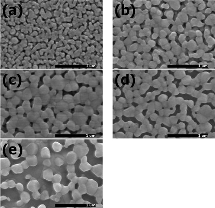
Figure 3 shows the FE-SEM images of Zn0.99Li0.01O films sintered at 600 ~ 1000 °C. The average grain sizes were 90 nm, 160 nm, 223 nm, 210 nm, and 250 nm, respectively. Corresponding sintering temperatures were 600 °C, 700 °C, 800 °C, 900 °C, and 1000 °C, respectively. As sintering temperatures were increased from 600 °C to 800 °C, the average grain sizes were increased. It is due to the grain growth of Zn0.99Li0.01O. At sintering temperature of 900 °C and 1000 °C, the grain size was decreased and then increased. It is thought to be due to the reduction of Zn0.99Li0.01O crystal quality and the emergences of new crystal phases. The new crystal phases included the phases of SiO2 cristobalite, and Li2SiO5.
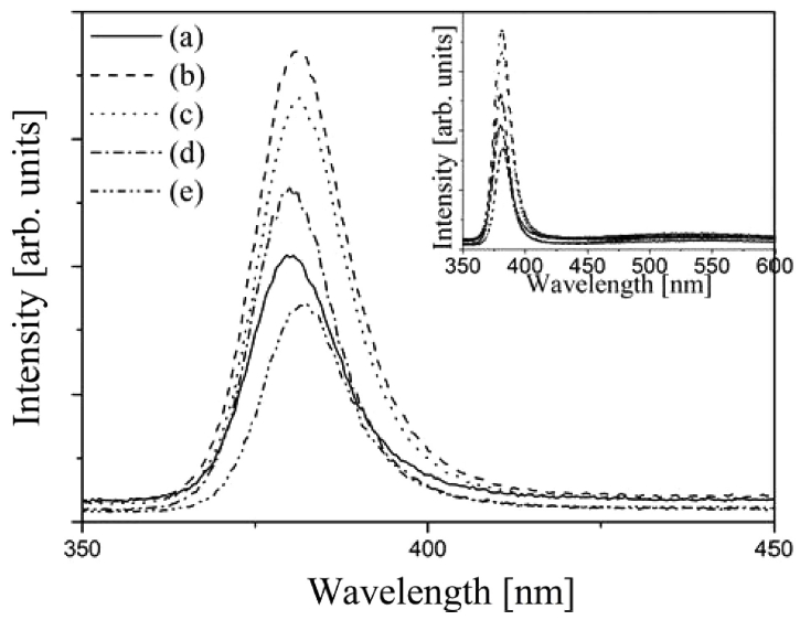
Figure 4 shows CL data for Zn0.99Li0.01O films sintered at various temperatures (600 ~ 1000 °C) measured at room temperature. Generally, two peaks known as UV and green emission are seen in the CL spectra in ZnO. It is well known that the origin of UV emission is the recombination of free exciton by an exciton-exciton collision process and that of green emission is explained by the oxygen vacancy. However, in this study, only UV emission peak (378.08 ~ 378.10 nm) was found in CL. In other words, the green emission did not appear, and the reason is considered with rich oxygen. The rich oxygen may be related to the annealing process in the air. According to calculated results of Xu [24], the origin of the green emission is the electron transition from shallow donor level formed by oxygen vacancies to shallow acceptor level by Zn vacancies. So if the mechanism was right, the intensity of green emission will decrease with the increment of oxygen. The air is rich in oxygen. In addition, Zhao et al. reported that green emissions were found in ZnO thin films that grew in vacuum, but for samples that grew under oxygen conditions, no green emissions were observed [25]. Therefore, if the samples were sintered in the air, oxygen vacancies may be significantly reduced. In fact, we investigated the O / Zn ratio of the sample using EDS (Energy Dispersive Spectrometry). As a result, the ratios of O / Zn are 1.52, 1.37, 1.42, 1.98, and 2.32 for each sample. Its corresponding sintering temperatures are 600, 700, 800, 900, and 1000 °C, respectively. According to these results, it found that the samples contained relatively high oxygen. Therefore, it is considered that the sufficient supply of oxygen during sintering process caused a reduction of the oxygen vacancy.
The UV emission peaks are located at 378.08, 378.22, and 378.23 nm for sintering temperatures of 600, 700, and 800 °C, respectively. A red shift of UV emission was found, which believed to be Burstein-Moss effect [26]. The Burstein-Moss effect is expressed in the following equation; ∆ E g = h 2 8 m * ( 3 π ) 2 / 3 n e 2 / 3
According to other studies, it showed that the emission peak's position for ZnO films changes by doping effect. Achilles et al. reported that as the doping concentration of Ag with ionic radii of 1.44Å increases, the UV emission changed from blue shift to red shift [27]. Qinghu et al. reported that blue shift was observed when Al with ionic radii of 0.54Å was doped [28]. A. Sa’asedi et al. reported that Li (0.76Å) doping has shown to cause the red shift of UV emission [29].
As sintering temperatures are increased, the Li ions are incorporated as substitutional acceptors into the structure rather than interstitial donors. In other words, the change in the UV emission peaks is related to the replacement of Zn by the smaller Li atom in the crystal by increased sintering temperature. It is supported by the decreased Zn0.99Li0.01O crystallite size as observed by XRD analysis (Fig 1, 2). The decrease in C-axis lattice constant means a decrease in the crystallite size. In addition, the red shift may be a result to obtain p-type ZnO by Li doping [30].
At sintering temperature of 900 °C, the position of UV emission peak was slightly moved toward the smaller wavelength. At sintering temperature of 1000 °C, the position of that was moved to the larger wavelength. This phenomenon may be due to the emergences of new crystal phases by increased sintering temperatures.
The relative intensity of the UV emission was increased from sintering temperature of 700 °C, and then decreased up to sintering temperature of 1000 °C. It is related to the quality of ZnO crystal. One of the important criteria for the crystal quality of ZnO films is FWHM of the (002) diffraction peak. The increased FWHM often means a decreased crystal quality. The values of FWHM were 0.35°, 0.25°, 0.26°, 0.34°, and 0.92° at sintering temperature of 600, 700, 800, 900, and 1000 °C, respectively. According to the results of FWHM and CL data, the quality of Zn0.99Li0.01O crystal was improved with increasing sintering temperature to 700 °C, and then worsened up to 1000 °C.
4. CONCLUSIONS
Zn0.99Li0.01O films were prepared on silicon substrates by using sol-gel method, and the prepared samples were sintered at various temperatures (600 °C ~1000 °C). From the XRD measurement, it is confirmed that the samples had the hexagonal phase of wurzite structure. However, new phases appeared in XRD patterns as sintering temperatures were increased. At sintering temperature of 800 °C, the SiO2 cristobalite phase was found. At the sintering temperature of 900 °C, the Li2SiO5 phase was appeared. It may be because of the diffusion of silicon atoms from silicon substrate by high sintering temperatures. In the CL measurement, the red shift of the UV emission was found. It may be because of the decrease of the carrier concentration by the Burstein-Moss effect. It is found that C-axis lattice constant was decreased with increasing temperatures. From these results, it is carefully concluded that the replacement of Zn by the smaller Li atom was increased with increasing sintering temperatures.