1. INTRODUCTION
Various transparent conductive oxide (TCO) films such as Sn-doped In2O3 (ITO) and Ga-doped ZnO (GZO) thin films are being used as transparent electrodes for large displays and thin-film solar cells [1,2]. Although conventional ITO thin film has high visible transmittance and low electrical resistivity, its optoelectrical applications are limited due to the rarity of indium (In), its poor mechanical properties, and chemical instabilities [3]. Thus, in recent years new metal oxide/metal/metal oxide (OMO) tri-layer films such as TiON/Au/TiON [4], ZTO/Ag/ZTO [5], and IGZO/Ni/IGZO [6] have been developed in the search for suitable candidates to replace conventional ITO films.
In this study, we propose the use of ZnO/Ag/SnO2 (ZAS) tri-layered films, with 50 nm thick ZnO and SnO2 thin films used as the metal oxide layers due to their mechanical hardness, abundance, chemical stability, and thermal stability; and 10 nm thick Ag thin film used as a metallic interlayer to act as an effective charge carrier. To investigate the optical and electrical properties of the films, ZnO 50 nm/Ag 10 nm/SnO2 50 nm films were deposited by RF and DC magnetron sputtering and then compared with a 100 nm thick SnO2 single layer film.
In addition, it is well known that post-deposition annealing of high quality TCO preparations increases their optical transmittance and electrical conductivity by enhancing the crystallinity of the films [8,9]. Thus, the effects of rapid thermal annealing in a low vacuum condition on the optical and electrical properties of the ZAS films was also investigated.
2. EXPERIMENTAL PROCEDURES
ZnO 50 nm/Ag 10 nm/SnO2 50 nm tri-layer films and 100 nm thick SnO2 single-layer films were deposited on a glass substrate (Corning 1797, 30 × 30 mm2) by RF and DC magnetron sputtering at room temperature, followed by postdeposition annealing, to compare their optical and electrical properties. Table 1 shows the experimental conditions of the magnetron sputtering and rapid thermal annealing (RTA) processes. The deposition rate and thickness of the films were measured with a surface profilometer (Dektak 500, Veeco). The surface roughness was evaluated via atomic force microscopy (XE-100, PSIA). A depth profile analysis was conducted with X-ray photoelectron spectroscopy at the Korea Basic Science Institute Busan center to observe the stacking structure of the film.
After post-deposition RTA, thin film crystallization was investigated with high-resolution X-ray diffraction (XRD; X’Pert Pro MRD, Philips) using Cu-Kα (0.154 nm) radiation. Optical transmittance (wavelength: 380–780 nm) and electrical properties such as the sheet resistance, carrier density and mobility of the films were measured with an ultraviolet-visible spectrophotometer (Cary100 Cone, Varian), four-point probe and Hall-effect measurement system (HMS-3000, Ecopia), respectively.
3. RESULTS AND DISCUSSION
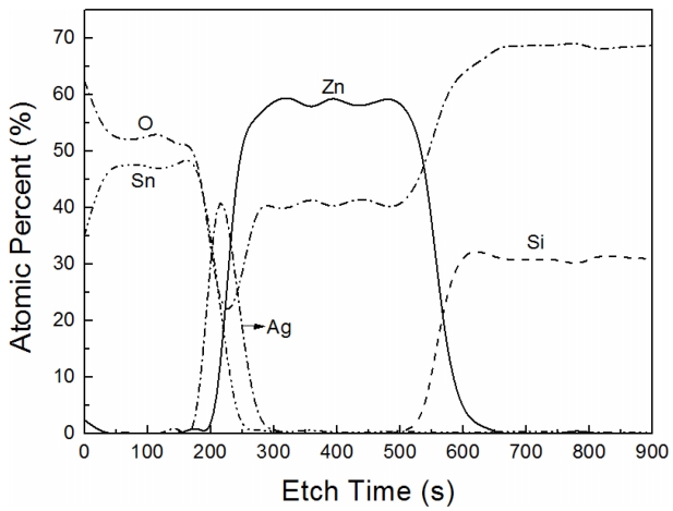
Figure 1 shows the X-ray photoelectron spectroscopy depth profile of as-deposited ZAS films, which consisted of tin (Sn) and oxygen at the surface, silver (Ag) in the middle, and zinc (Zn) and oxygen on the bottom.
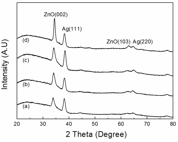
Figure 2 shows the XRD patterns of the as-deposited (Fig. 2a) and the rapid thermal annealed ZAS films (Figs. 2b-d). The observed diffraction peaks are related to the ZnO (JCPDS card; 36-1451) and the bottom layer and Ag (JCPDS card; 87-0719) interlayer, respectively. The XRD pattern indicated that the ZnO films had a C-axis orientation. The peak intensity of the XRD pattern related to the ZnO (002) peak of the annealed films was higher than that of the asdeposited film; in addition, the full width at half-maximum (FWHM) of the ZnO (002) diffraction peak for the annealed films was smaller than that of the as-deposited ZnO film. Therefore, the crystallinity of the ZnO was improved by rapid annealing [7].
However, crystallization of the Ag interlayer and SnO2 surface layer were not significantly affected by the annealing temperature, compared with the ZnO bottom layer. As shown in Fig. 2, the annealed films did not show any change in the FWHM of the Ag (111) diffraction peak; furthermore, no diffraction peaks related to the SnO2 film can be observed in the XRD pattern. Therefore, the 50-nm-thick SnO2 upper film remained amorphous regardless of the annealing temperature.
Table 2 shows the grain size of both the ZnO (002) and Ag (111) planes as evaluated by the Scherrer equation [7]. The grain size of the ZnO bottom layer increased proportionally to the annealing temperature. In a previous study, Kim [8] reported that the optical and electrical properties of TCO films depended on the crystallinity of the films, because the grain boundary can simultaneously absorb visible light and decrease carrier mobility. Because enlarged grain size results in a decreased absorption of visible light, the visible transmittance of the films is expected to increase with annealing temperature.
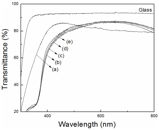
Figure 3 shows the optical transmittance of ZAS films annealed at different temperatures. The average visible transmittance of the as-deposited ZAS films was approximately 80.8%. After annealing at 450 °C, the ZAS films showed an increased transmittance of 82.4% due to grain growth, as shown Table 2.
Table 3 shows the electrical properties of the as-deposited SnO2 films and ZAS films as a function of annealing temperature. The films annealed at 450 °C had the lowest resistivity of 7.0 × 10⁻⁵ Ω cm, due to an enhanced carrier mobility of 13.1 cm2 V-1S-1.
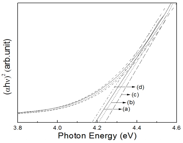
Figure 4 shows a plot of (αhν)2 in the ZAS films as a function of photon energy. The optical absorption coefficient (α) can be calculated from the following equation (1) [8]:
Here, d is the film thickness and T is the visible transmittance. The Tauc formula (2) gives the relationship between the optical absorption coefficient (α) and optical band gap (Eg) [9]:
Here, hν is the energy of the incident photon and A is the absorption edge width parameter [10]. In Fig. 4, as the annealing temperature increases to 300 °C, the optical band gap increases proportionally from 4.19 eV (at deposition) to 4.24 eV (at 300 °C). From the observed electrical properties and optical band gap, it can be concluded that the broadening of the optical band gap is related to the increased carrier density of the film. The band gap increased from 4.19 eV to 4.24 eV, with the carrier density increasing from 7.09 × 1021 cm−3 to 7.77 × 1021 cm−3. However, the film annealed at 450 °C showed a decrease in band gap energy of 4.17 eV due to the decreased carrier density of 6.80 × 1021 cm−3. It is supposed that the surface oxidation decreased the carrier density during thermal annealing at 450 °C. Recently, Tang [10] reported similar results for band gap shift, which depended on the electron density of the GZO thin film.
4. CONCLUSIONS
In this study, ZnO 50 nm/Ag 10 nm/SnO2 50 nm (ZAS) trilayer films and 100 nm thick SnO2 single layer films were deposited by RF and DC magnetron sputtering and then underwent rapid thermal annealing. Measurements were conducted to determine the usefulness of ZAS film as a transparent electrode and the effects of annealing temperature on the structural, optical, and electrical properties of the ZAS films.
As-deposited ZAS films exhibited a visible transmittance of 80.8%, which was comparable to that of SnO2 films but has a lower resistivity of 1.2 × 10⁻⁴ Ω cm compared to SnO2 films. After post-deposition rapid thermal annealing at 450 °C, ZAS films showed an enhanced optical transmittance of 82.4% and a lower resistivity of 7.0 × 10⁻⁵ Ω cm. The results indicate that rapid thermal annealed ZAS film with a 10 nm thick Ag interlayer is a possible candidate for use as a transparent electrode in various display devices.


